


PRELIMINARY CY8CNP102B, CY8CNP102E
Document #: 001-43991 Rev. *D Page 18 of 38
In the following table, t
HRECALL
starts from the time Vcc rises above V
SWITCH.
If an SRAM WRITE has not taken place since the last
nonvolatile cycle, no STORE occurs. Industrial grade devices require 15 ms maximum.
AC General Purpose IO Specifications
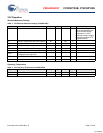
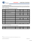
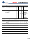
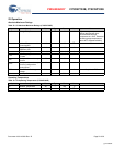
Table 15.3.3V nvSRAM AutoStore/Power Up RECALL (CY8CNP102B)
Parameter Description
nvSRAM
Unit
Min Max
t
HRECALL
Power Up RECALL Duration 20 ms
t
STORE
STORE Cycle Duration 12.5 ms
V
SWITCH
Low Voltage Trigger Level 2.65 V
t
VccRISE
VCC Rise Time 150 μs
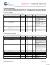
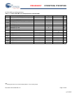
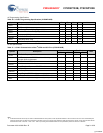
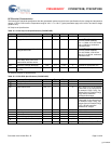
Table 16. 3.3V AC GPIO Specifications (CY8CNP102B)
Symbol Description Min Typ Max Units Notes
F
GPIO
GPIO Operating Frequency 0 – 12.3 MHz Normal Strong Mode
TRiseS Rise Time, Slow Strong Mode, Cload = 50 pF 10 27 – ns Vcc = 3V to 3.6V
10% - 90%
TFallS Fall Time, Slow Strong Mode, Cload = 50 pF 10 22 – ns Vcc = 3V to 3.6V
10% - 90%
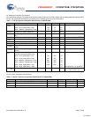
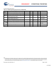
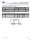
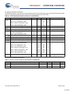
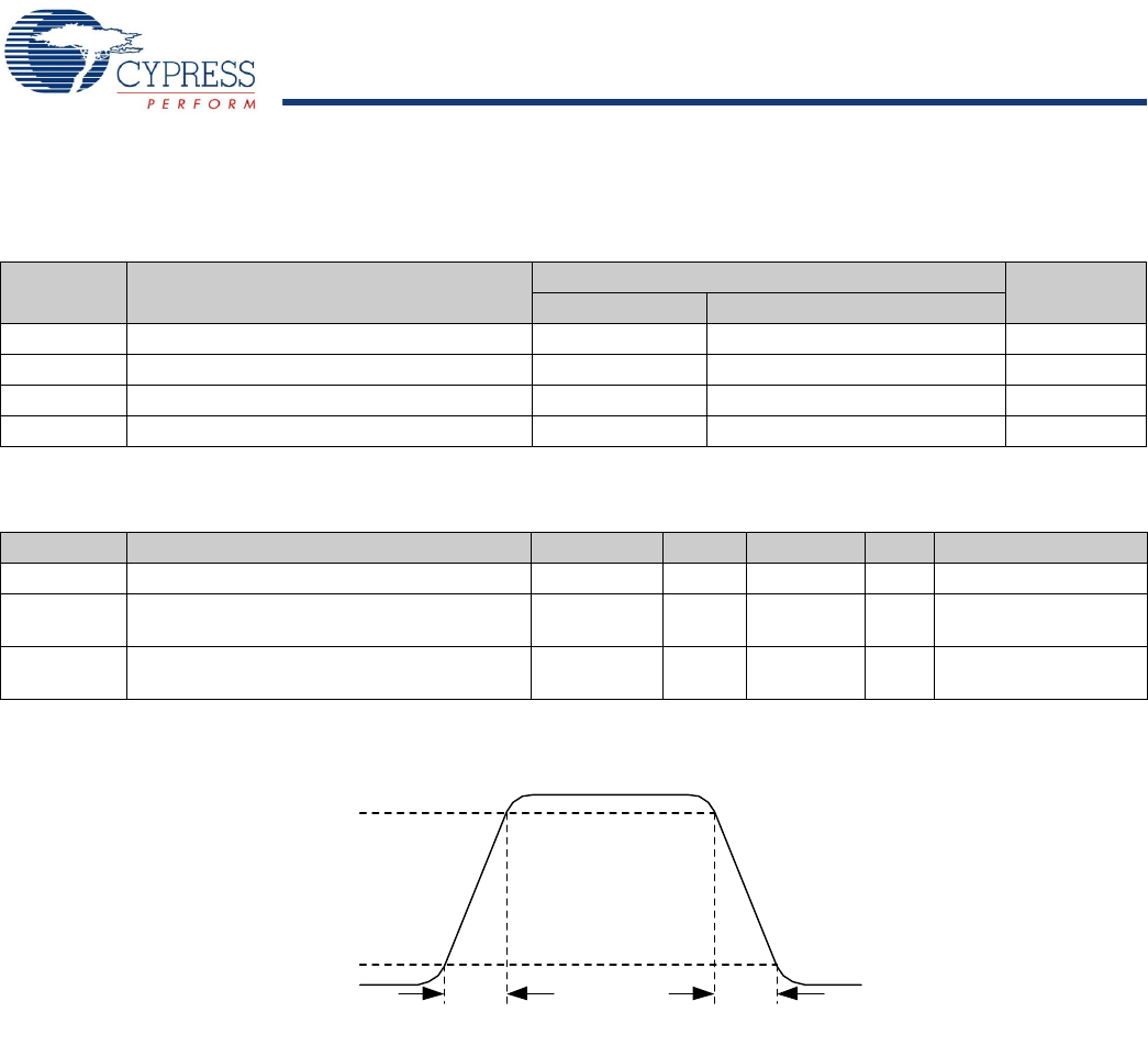
Figure 6. GPIO Timing Diagram
TFallF
TFallS
TRiseF
TRiseS
90%
10%
GPIO
Pin
Output
Voltage
[+] Feedback