


PRELIMINARY CY8CNP102B, CY8CNP102E
Document #: 001-43991 Rev. *D Page 4 of 38
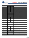
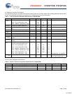
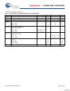
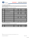
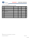
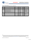
18 P5_7 IO GPIO
19 P5_5 IO GPIO
20 P5_3 IO GPIO
21 P5_1 IO GPIO
22 P1_7 IO I2C Serial Clock (SCL), GPIO
23 P1_5 IO I2C Serial Data (SDA), GPIO
24 P1_3 IO GPIO
25 P1_1 IO Serial Clock (SCL), Crystal (XTALin), GPIO
26 NV_W Connect to pin 16 (NV_W to EN_W)
27 - 34 NC
Not connected on the die
35 - 39 Vss Power Ground
40 - 47 NC
Not connected on the die
48 DNU Reserved for test modes - Do Not Use
49 NV_A1 Connect to pin 58 (NV_A1 to EN_A1)
50 NV_A2 Connect to pin 59 (NV_A2 to EN_A2)
51 P1_0 IO Serial Data (SDA), Crystal (XTALout), GPIO
52 P1_2 IO GPIO
53 P1_6 IO GPIO
54 P5_0 IO GPIO
55 P5_2 IO GPIO
56 P5_4 IO GPIO
57 P5_6 IO GPIO
58 EN_A1 Connect to Pin 49 (EN_A1 to NV_A1)
59 EN_A2 Connect to Pin 50 (EN_A2 to NV_A2)
60 EN_O Connect to Pin 76 (EN_O to NV_O)
61 EN_C Connect to Pin 99 (EN_C to NV_C)
62 XRES Input Active high external reset (Internal Pull down)
63 VCAP Power External Capacitor connection for nvSRAM
64 Vcc Power Supply Voltage
65 P2_0 IO I Direct Switched Capacitor Block Input, GPIO
66 P2_2 IO I Direct Switched Capacitor Block Input, GPIO
67 P2_4 IO External Analog GND, GPIO
68 P2_6 IO External Voltage Ref, GPIO
69 P0_0 IO I Analog Column Mux Input, GPIO
70 P0_2 IO IO Analog Column Mux Input and Column Output
71 P0_4 IO IO Analog Column Mux Input and Column Output
72-73 NC
Not connected on the die
74 P0_6 IO I Analog Column Mux Input, GPIO
75 Vcc Power Supply Voltage
76 NV_O Connect to Pin 60 (NV_O to EN_O)
77 DNU Reserved for test modes - Do Not Use
78 NC
Not connected on the die
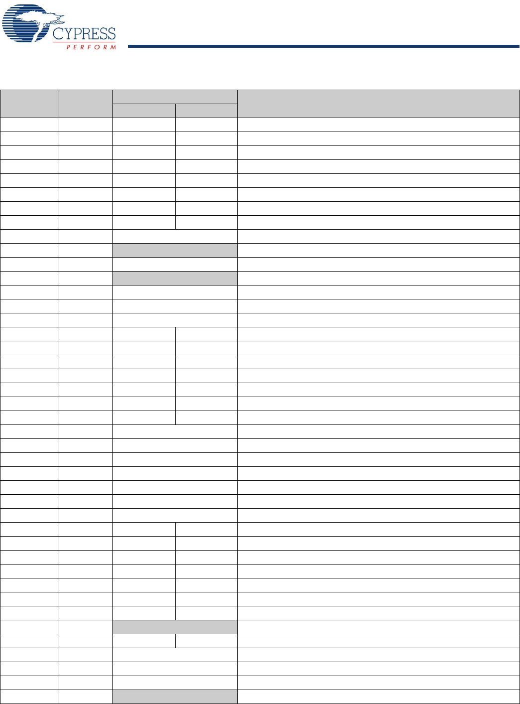
Table 1. Pin Definitions - 100-Pin TQFP (continued)
Pin Number Pin Name
Type
Pin Definition
Digital Analog
[+] Feedback