


PRELIMINARY CY8CNP102B, CY8CNP102E
Document #: 001-43991 Rev. *D Page 29 of 38
In the following table, t
HRECALL
starts from the time Vcc rises above V
SWITCH.
If an SRAM WRITE has not taken place since the last
nonvolatile cycle, no STORE takes place. Industrial grade devices require 15 ms maximum.
AC General Purpose IO Specifications
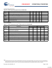
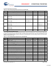
Table 34. 5V nvSRAM AutoStore/Power Up RECALL (CY8CNP102E)
Parameter Description
nvSRAM
Unit
Min Max
t
HRECALL
Power Up RECALL Duration 20 ms
t
STORE
STORE Cycle Duration 12.5 ms
V
SWITCH
Low Voltage Trigger Level 4.4 V
t
VccRISE
VCC Rise Time 150 μs
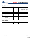
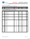
Table 35. 5V AC GPIO Specifications (CY8CNP102E)
Symbol Description Min Typ Max Units Notes
F
GPIO
GPIO Operating Frequency 0 – 12.3 MHz Normal Strong Mode
TRiseF Rise Time, Normal Strong Mode, Cload = 50 pF 3 – 18 ns Vcc = 4.75V to 5.25V
10% - 90%
TFallF Fall Time, Normal Strong Mode, Cload = 50 pF 2 – 18 ns Vcc = 4.75V to 5.25V
10% - 90%
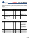
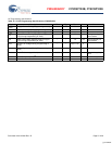
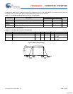
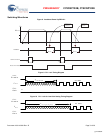
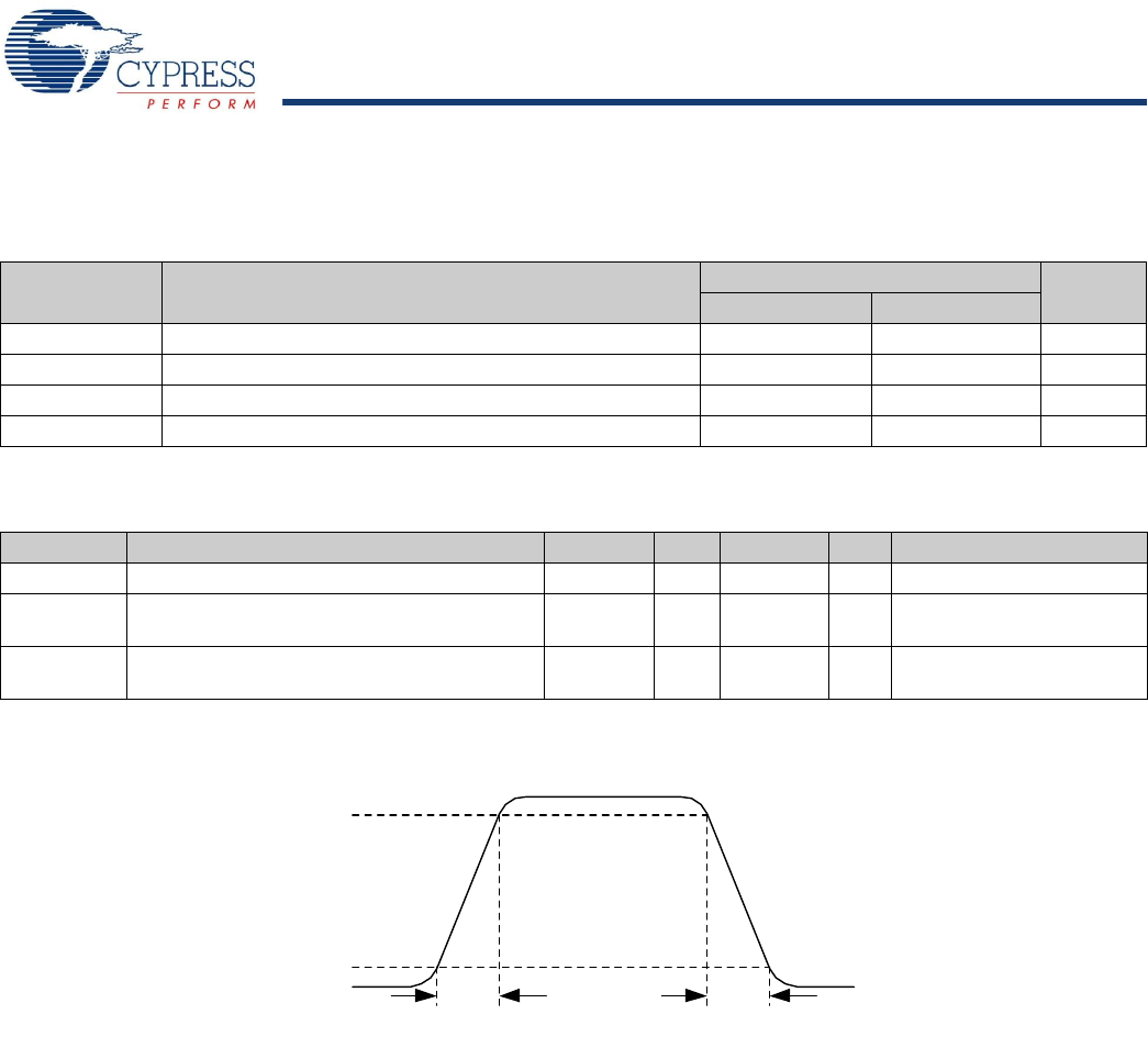
Figure 7. GPIO Timing Diagram
TFallF
TFallS
TRiseF
TRiseS
90%
10%
GPIO
Pin
Output
Voltage
[+] Feedback