


PRELIMINARY CY8CNP102B, CY8CNP102E
Document #: 001-43991 Rev. *D Page 26 of 38
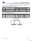
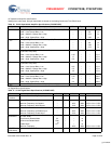
DC Analog PSoC NV Block Specifications
DC POR, SMP, and LVD Specifications
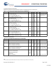
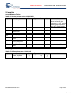
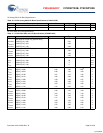
Table 30. 5V DC Analog PSoC NV Block Specifications (CY8CNP102E)
Symbol Description Min Typ Max Units
R
CT
Resistor Unit Value (Continuous Time) – 12.2 – kΩ
C
SC
Capacitor Unit Value (Switch Cap) – 80 – fF
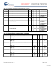
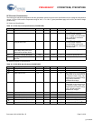
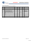
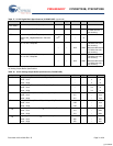
Table 31. 5V DC POR, SMP, and LVD Specifications (CY8CNP102E)
Symbol Description Min Typ Max Units
Vdd Value for PPOR Trip (positive ramp)
V
PPOR0R
PORLEV[1:0] = 00b 2.91 V
V
PPOR1R
PORLEV[1:0] = 01b 4.39 V
V
PPOR2R
PORLEV[1:0] = 10b 4.55 V
Vdd Value for PPOR Trip (negative ramp)
V
PPOR0
PORLEV[1:0] = 00b 2.82 V
V
PPOR1
PORLEV[1:0] = 01b 4.39 V
V
PPOR2
PORLEV[1:0] = 10b 4.55 V
PPOR Hysteresis
V
PH0
PORLEV[1:0] = 00b 92 mV
V
PH1
PORLEV[1:0] = 01b 0 mV
V
PH2
PORLEV[1:0] = 10b 0 mV
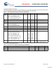
Vdd Value for LVD Trip
V
LVD0
VM[2:0] = 000b 2.86 2.92 2.98
[2]
V
V
LVD1
VM[2:0] = 001b 2.96 3.02 3.08 V
V
LVD2
VM[2:0] = 010b 3.07 3.13 3.20 V
V
LVD3
VM[2:0] = 011b 3.92 4.00 4.08 V
V
LVD4
VM[2:0] = 100b 4.39 4.48 4.57 V
V
LVD5
VM[2:0] = 101b 4.55 4.64 4.74 V
V
LVD6
VM[2:0] = 110b 4.63 4.73 4.82 V
V
LVD7
VM[2:0] = 111b 4.72 4.81 4.91 V
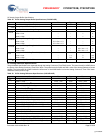
Vdd Value for SMP Trip
V
PUMP0
VM[2:0] = 000b 2.96 3.02 3.08 V
V
PUMP1
VM[2:0] = 001b 3.03 3.10 3.16 V
V
PUMP2
VM[2:0] = 010b 3.18 3.25 3.32 V
V
PUMP3
VM[2:0] = 011b 4.11 4.19 4.28 V
V
PUMP4
VM[2:0] = 100b 4.55 4.64 4.74 V
V
PUMP5
VM[2:0] = 101b 4.63 4.73 4.82 V
V
PUMP6
VM[2:0] = 110b 4.72 4.82 4.91 V
V
PUMP7
VM[2:0] = 111b 4.90 5.00 5.10 V
[+] Feedback