5V, 3.3V, ISR™ High-Performance CPLDs
Ultra37000 CPLD Family
Cypress Semiconductor Corporation • 3901 North First Street • San Jose, CA 95134 • 408-943-2600
Document #: 38-03007 Rev. *E Revised March 7, 2004
Features
• In-System Reprogrammable™ (ISR™) CMOS CPLDs
— JTAG interface for reconfigurability
— Design changes do not cause pinout changes
— Design changes do not cause timing changes
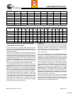
• High density
— 32 to 512 macrocells
— 32 to 264 I/O pins
— Five dedicated inputs including four clock pins
• Simple timing model
— No fanout delays
— No expander delays
— No dedicated vs. I/O pin delays
— No additional delay through PIM
— No penalty for using full 16 product terms
— No delay for steering or sharing product terms
• 3.3V and 5V versions
• PCI-compatible
[1]
• Programmable bus-hold capabilities on all I/Os
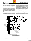
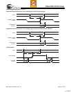
• Intelligent product term allocator provides:
— 0 to 16 product terms to any macrocell
— Product term steering on an individual basis
— Product term sharing among local macrocells
• Flexible clocking
— Four synchronous clocks per device
— Product term clocking
— Clock polarity control per logic block
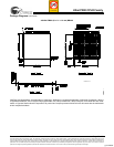
• Consistent package/pinout offering across all densities
— Simplifies design migration
— Same pinout for 3.3V and 5.0V devices
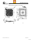
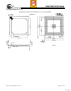
• Packages
— 44 to 400 leads in PLCC, CLCC, PQFP, TQFP, CQFP,
BGA, and Fine-Pitch BGA packages
— Lead (Pb)-free packages available
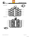
General Description
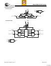
The Ultra37000™ family of CMOS CPLDs provides a range of
high-density programmable logic solutions with unparalleled
system performance. The Ultra37000 family is designed to
bring the flexibility, ease of use, and performance of the 22V10
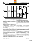
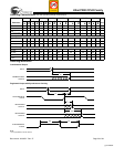
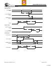
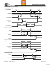
to high-density CPLDs. The architecture is based on a number
of logic blocks that are connected by a Programmable Inter-
connect Matrix (PIM). Each logic block features its own
product term array, product term allocator, and 16 macrocells.
The PIM distributes signals from the logic block outputs and all
input pins to the logic block inputs.
All of the Ultra37000 devices are electrically erasable and
In-System Reprogrammable (ISR), which simplifies both
design and manufacturing flows, thereby reducing costs. The
ISR feature provides the ability to reconfigure the devices
without having design changes cause pinout or timing
changes. The Cypress ISR function is implemented through a
JTAG-compliant serial interface. Data is shifted in and out
through the TDI and TDO pins, respectively. Because of the
superior routability and simple timing model of the Ultra37000
devices, ISR allows users to change existing logic designs
while simultaneously fixing pinout assignments and
maintaining system performance.
The entire family features JTAG for ISR and boundary scan,
and is compatible with the PCI Local Bus specification,
meeting the electrical and timing requirements. The
Ultra37000 family features user programmable bus-hold
capabilities on all I/Os.
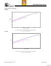
Ultra37000 5.0V Devices
The Ultra37000 devices operate with a 5V supply and can
support 5V or 3.3V I/O levels. V
CCO
connections provide the
capability of interfacing to either a 5V or 3.3V bus. By
connecting the V
CCO
pins to 5V the user insures 5V TTL levels
on the outputs. If V
CCO
is connected to 3.3V the output levels
meet 3.3V JEDEC standard CMOS levels and are 5V tolerant.
These devices require 5V ISR programming.
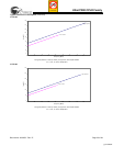
Ultra37000V 3.3V Devices
Devices operating with a 3.3V supply require 3.3V on all V
CCO
pins, reducing the device’s power consumption. These
devices support 3.3V JEDEC standard CMOS output levels,
and are 5V-tolerant. These devices allow 3.3V ISR
programming.
Note:
1. Due to the 5V-tolerant nature of 3.3V device I/Os, the I/Os are not clamped to V
CC
, PCI V
IH
= 2V.
[+] Feedback