Ultra37000 CPLD Family
Document #: 38-03007 Rev. *E Page 7 of 64
JTAG and PCI Standards
PCI Compliance
5V operation of the Ultra37000 is fully compliant with the PCI
Local Bus Specification published by the PCI Special Interest
Group. The 3.3V products meet all PCI requirements except
for the output 3.3V clamp, which is in direct conflict with 5V
tolerance. The Ultra37000 family’s simple and predictable
timing model ensures compliance with the PCI AC specifica-
tions independent of the design.
IEEE 1149.1-compliant JTAG
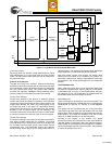
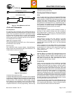
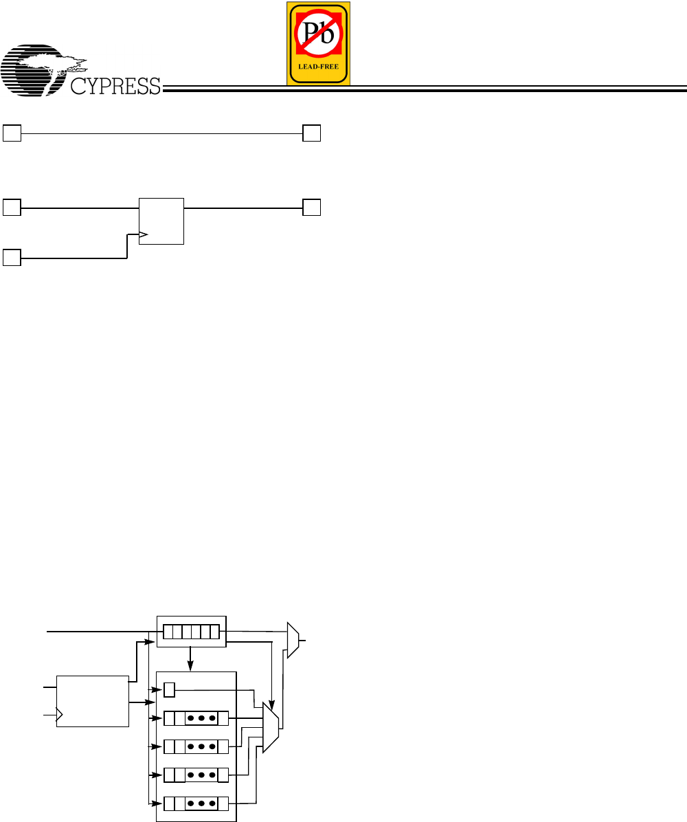
The Ultra37000 family has an IEEE 1149.1 JTAG interface for
both Boundary Scan and ISR.
Boundary Scan
The Ultra37000 family supports Bypass, Sample/Preload,
Extest, Idcode, and Usercode boundary scan instructions. The
JTAG interface is shown in Figure 6.
In-System Reprogramming (ISR)
In-System Reprogramming is the combination of the capability
to program or reprogram a device on-board, and the ability to
support design changes without changing the system timing
or device pinout. This combination means design changes
during debug or field upgrades do not cause board respins.
The Ultra37000 family implements ISR by providing a JTAG
compliant interface for on-board programming, robust routing
resources for pinout flexibility, and a simple timing model for
consistent system performance.
Development Software Support
Warp
Warp is a state-of-the-art compiler and complete CPLD design
tool. For design entry, Warp provides an IEEE-STD-1076/1164
VHDL text editor, an IEEE-STD-1364 Verilog text editor, and a
graphical finite state machine editor. It provides optimized
synthesis and fitting by replacing basic circuits with ones
pre-optimized for the target device, by implementing logic in
unused memory and by perfect communication between fitting
and synthesis. To facilitate design and debugging, Warp
provides graphical timing simulation and analysis.
Warp Professional
™
Warp Professional contains several additional features. It
provides an extra method of design entry with its graphical
block diagram editor. It allows up to 5 ms timing simulation
instead of only 2 ms. It allows comparison of waveforms before
and after design changes.
Warp Enterprise
™
Warp Enterprise provides even more features. It provides
unlimited timing simulation and source-level behavioral
simulation as well as a debugger. It has the ability to generate
graphical HDL blocks from HDL text. It can even generate
testbenches.
Warp is available for PC and UNIX platforms. Some features
are not available in the UNIX version. For further information
see the Warp for PC, Warp for UNIX, Warp Professional and
Warp Enterprise data sheets on Cypress’s web site
(www.cypress.com).
Third-Party Software
Although Warp is a complete CPLD development tool on its
own, it interfaces with nearly every third party EDA tool. All
major third-party software vendors provide support for the
Ultra37000 family of devices. Refer to the third-party software
data sheet or contact your local sales office for a list of
currently supported third-party vendors.
Programming
There are four programming options available for Ultra37000
devices. The first method is to use a PC with the 37000
UltraISR programming cable and software. With this method,
the ISR pins of the Ultra37000 devices are routed to a
connector at the edge of the printed circuit board. The 37000
UltraISR programming cable is then connected between the
parallel port of the PC and this connector. A simple configu-
ration file instructs the ISR software of the programming
operations to be performed on each of the Ultra37000 devices
in the system. The ISR software then automatically completes
all of the necessary data manipulations required to accomplish
the programming, reading, verifying, and other ISR functions.
For more information on the Cypress ISR Interface, see the
ISR Programming Kit data sheet (CY3700i).
The second method for programming Ultra37000 devices is on
automatic test equipment (ATE). This is accomplished through
a file created by the ISR software. Check the Cypress website
for the latest ISR software download information.
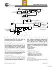
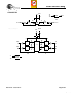
Figure 5. Timing Model for CY37128
Figure 6. JTAG Interface
COMBINATORIAL SIGNAL
REGISTERED SIGNAL
D,T,L O
CLOCK
INPUT
INPUT
OUTPUT
OUTPUT
t
S
= 3.5 ns
t
CO
= 4.5 ns
t
PD
= 6.5 ns
Instruction Register
Boundary Scan
idcode
Usercode
ISR Prog.
Bypass Reg.
Data Registers
JTAG
TAP
CONTROLLER
TDO
TDI
TMS
TCK
[+] Feedback


