


Ultra37000 CPLD Family
Document #: 38-03007 Rev. *E Page 6 of 64
Clocking
Each I/O and buried macrocell has access to four synchronous
clocks (CLK0, CLK1, CLK2 and CLK3) as well as an
asynchronous product term clock PTCLK. Each input
macrocell has access to all four synchronous clocks.
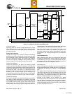
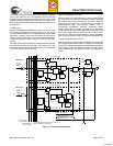
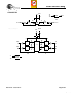
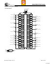
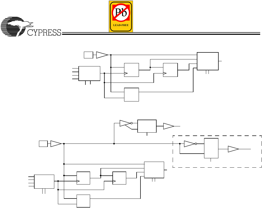
Dedicated Inputs/Clocks
Five pins on each member of the Ultra37000 family are desig-
nated as input-only. There are two types of dedicated inputs
on Ultra37000 devices: input pins and input/clock pins.
Figure 3 illustrates the architecture for input pins. Four input
options are available for the user: combinatorial, registered,
double-registered, or latched. If a registered or latched option
is selected, any one of the input clocks can be selected for
control.
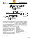
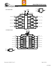
Figure 4 illustrates the architecture for the input/clock pins.
Like the input pins, input/clock pins can be combinatorial,
registered, double-registered, or latched. In addition, these
pins feed the clocking structures throughout the device. The
clock path at the input has user-configurable polarity.
Product Term Clocking
In addition to the four synchronous clocks, the Ultra37000
family also has a product term clock for asynchronous
clocking. Each logic block has an independent product term
clock which is available to all 16 macrocells. Each product term
clock also supports user configurable polarity selection.
Timing Model
One of the most important features of the Ultra37000 family is
the simplicity of its timing. All delays are worst case and
system performance is unaffected by the features used.
Figure 5 illustrates the true timing model for the 167-MHz
devices in high speed mode. For combinatorial paths, any
input to any output incurs a 6.5-ns worst-case delay regardless
of the amount of logic used. For synchronous systems, the
input set-up time to the output macrocells for any input is 3.5
ns and the clock to output time is also 4.0 ns. These measure-
ments are for any output and synchronous clock, regardless
of the logic used.
The Ultra37000 features:
• No fanout delays
• No expander delays
• No dedicated vs. I/O pin delays
• No additional delay through PIM
• No penalty for using 0–16 product terms
• No added delay for steering product terms
• No added delay for sharing product terms
• No routing delays
• No output bypass delays
The simple timing model of the Ultra37000 family eliminates
unexpected performance penalties.
Figure 3. Input Macrocell
0
1
2
3
O
C12 C13
TO PIM
D
Q
D
Q
D
Q
LE
INPUT PIN
0
1
2
O
C10
FROM CLOCK
POLARITY MUXES
3
C11
Figure 4. Input/Clock Macrocell
0
1
2
3
O
C10C11
TO PIM
D
Q
D
Q
D
Q
LE
INPUT/CLOCK PIN
0
1
2
O
FROM CLOCK
CLOCK PINS
0
1
O
C12
TO CLOCK MUX ON
ALL INPUT MACROCELLS
TO CLOCK MUX
IN EACH
3
0
1
CLOCK POLARITY MUX
ONE PER LOGIC BLOCK
FOR EACH CLOCK INPUT
POLARITY INPUT
LOGIC BLOCK
C8
C9
C13, C14, C15 OR C16
O
[+] Feedback