


Ultra37000 CPLD Family
Document #: 38-03007 Rev. *E Page 15 of 64
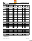
3.3V Device Characteristics
Maximum Ratings
(Above which the useful life may be impaired. For user guide-
lines, not tested.)
Storage Temperature .................................–65°C to +150°C
Ambient Temperature with
Power Applied.............................................–55°C to +125°C
Supply Voltage to Ground Potential............... –0.5V to +4.6V
DC Voltage Applied to Outputs
in High-Z State................................................–0.5V to +7.0V
DC Input Voltage ............................................–0.5V to +7.0V
DC Program Voltage.............................................3.0 to 3.6V
Current into Outputs ......................................................8 mA
Static Discharge Voltage...........................................> 2001V
(per MIL-STD-883, Method 3015)
Latch-up Current.....................................................> 200 mA
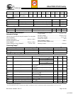
Inductance
[5]
Parameter Description Test Conditions
44-Lead
TQFP
44-Lead
PLCC
44-Lead
CLCC
84-Lead
PLCC
84-Lead
CLCC
100-Lead
TQFP
160-Lead
TQFP
208-Lead
PQFP Unit
L Maximum Pin
Inductance
V
IN
= 5.0V
at f = 1 MHz
25285 8 911nH
Capacitance
[5]
Parameter Description Test Conditions Max. Unit
C
I/O
Input/Output Capacitance V
IN
= 5.0V at f = 1 MHz at T
A
= 25°C 10 pF
C
CLK
Clock Signal Capacitance V
IN
= 5.0V at f = 1 MHz at T
A
= 25°C 12 pF
C
DP
Dual-Function Pins
[9]
V
IN
= 5.0V at f = 1 MHz at T
A
= 25°C 16 pF
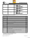
Endurance Characteristics
[5]
Parameter Description Test Conditions Min. Typ. Unit
N Minimum Reprogramming Cycles Normal Programming Conditions
[2]
1,000 10,000 Cycles
Operating Range
[2]
Range Ambient Temperature
[2]
Junction Temperature V
CC
[10]
Commercial 0°C to +70°C 0°C to +90°C 3.3V ± 0.3V
Industrial –40°C to +85°C –40°C to +105°C 3.3V ± 0.3V
Military
[3]
–55°C to +125°C –55°C to +130°C 3.3V ± 0.3V
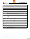
3.3V Device Electrical Characteristics Over the Operating Range
Parameter Description Test Conditions Min. Max. Unit
V
OH
Output HIGH Voltage V
CC
= Min. I
OH
= –4 mA (Com’l)
[4]
2.4 V
I
OH
= –3 mA (Mil)
[4]
V
OL
Output LOW Voltage V
CC
= Min. I
OL
= 8 mA (Com’l)
[4]
0.5 V
I
OL
= 6 mA (Mil)
[4]
V
IH
Input HIGH Voltage Guaranteed Input Logical HIGH Voltage for
all Inputs
[7]
2.0 5.5 V
V
IL
Input LOW Voltage Guaranteed Input Logical LOW Voltage for
all Inputs
[7]
–0.5 0.8 V
I
IX
Input Load Current V
I
= GND OR V
CC
, Bus-Hold Disabled –10 10 µA
I
OZ
Output Leakage Current V
O
= GND or V
CC
, Output Disabled,
Bus-Hold Disabled
–50 50 µA
I
OS
Output Short Circuit Current
[5, 8]
V
CC
= Max., V
OUT
= 0.5V –30 –160 mA
I
BHL
Input Bus-Hold LOW Sustaining Current V
CC
= Min., V
IL
= 0.8V +75 µA
I
BHH
Input Bus-Hold HIGH Sustaining Current V
CC
= Min., V
IH
= 2.0V –75 µA
I
BHLO
Input Bus-Hold LOW Overdrive Current V
CC
= Max. +500 µA
I
BHHO
Input Bus-Hold HIGH Overdrive Current V
CC
= Max. –500 µA
Notes:
9. Dual pins are I/O with JTAG pins.
10.For CY37064VP100-143AC, CY37064VP100-143BBC, CY37064VP44-143AC, CY37064VP48-143BAC; Operating Range: V
CC
is 3.3V± 0.16V.
[+] Feedback