


EM78P458/459
OTP ROM
0 = The Vref of the ADC is connected to Vdd (default value), and the P53/VREF pin carries out
the function of P53;
1 = The Vref of the ADC is connected to P53/VREF.
• CE (Bit 6): Control bit used to enable comparator.
0 = Disable comparator
1 = Enable comparator
• COE (Bit 5): Set P57 as the output of the comparator
0 = the comparator acts as an OP if CE=1.
1 = act as a comparator if CE=1.
• IMS2~IMS0 (Bit 4 ~ Bit 2): ADC configuration definition bit.
• CKR1 and CKR0 (Bit 1 and Bit 0): The conversion time select.
00 = Fosc/4;
01 = Fosc/16;
10 = Fsco/64;
11 = The oscillator clock source of ADC is from WDT ring oscillator frequency.
( frequency=256/18ms≒14.2Khz)
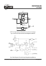
1.3 GCON/IOC90
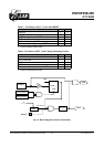
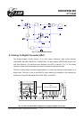
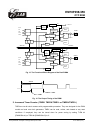
As shown in Fig. 12, OP1 and OP2, the gain amplifiers, are located in the middle of the analog
input pins (ADC1 and ADC5) and the 8-1analog switch. The GCON register controls the gains.
Table 7 Table 7 Sho
ws the Gains and the Operating Range of ADC.
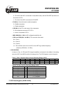
BIT 7 6 5 4 3 2 1 0
SYMBOL OP2E OP1E G22 G21 G20 G12 G11 G10
*Init_Value 0 0 0 0 0 0 0 0
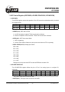
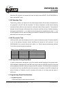
Table 8 The Gains and the Operating Range of ADC
G10:G12/G20:G22 Gain Range of Operating Voltage
000 1 0 ~ Vref
001 2 0 ~ (1/2)Vref
010 4 0 ~ (1/4)Vref
011 8 0 ~ (1/8)Vref
100 16 0 ~ (1/16)Vref
101 32 0 ~ (1/32)Vref
<Note> Vref can not be less than 3 volts.
2. ADC Data Register (ADDATA/RA)
This specification is subject to change without prior notice. 07.01.2003 (V1.3)
33