RX − 8564 LC
Page − 11
ETM12E-01
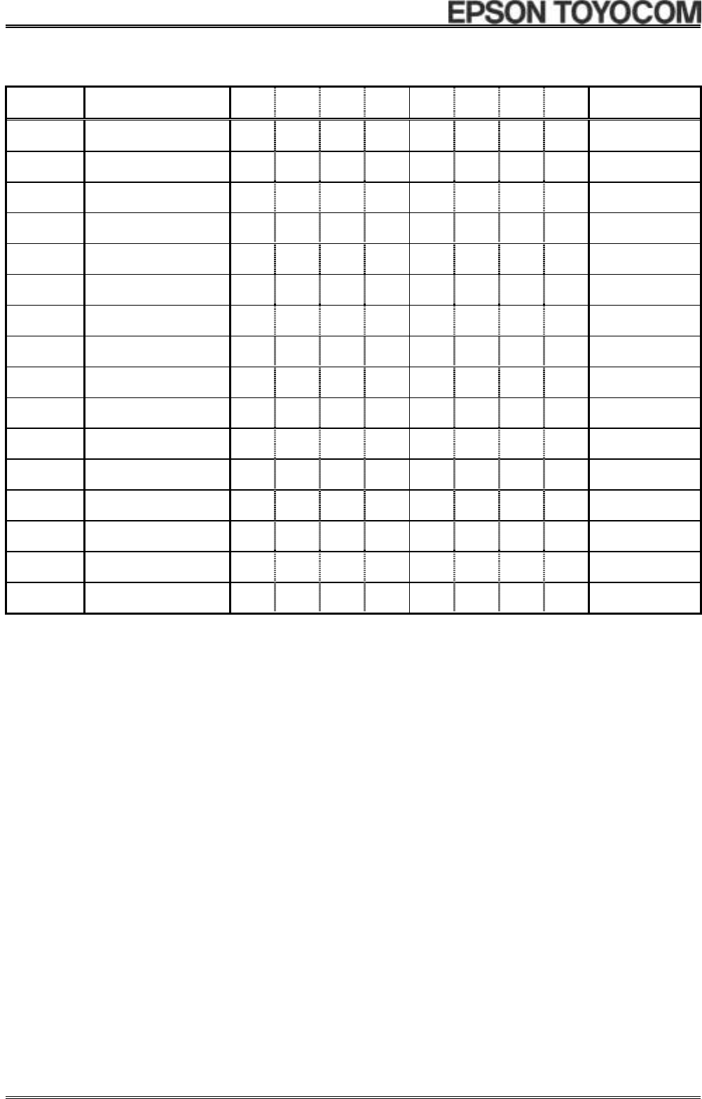
12.2. Register table
Address [h]
Function bit 7 bit 6 bit 5 bit 4 bit 3 bit 2 bit 1 bit 0 note
00 Control 1 TEST 0 STOP 0 TEST 0 0 0
∗3 , ∗4
01 Control 2 0
×
0
TI / TP
AF TF AIE TIE
∗4 , ∗5
02 Seconds VL 40 20 10 8 4 2 1
∗1
03 Minutes
×
40 20 10 8 4 2 1
∗5
04 Hours
× ×
20 10 8 4 2 1
∗5
05 Days
× ×
20 10 8 4 2 1
∗5
06 Weekdays
× × × × ×
4 2 1
∗5
07 Months / Century C
× ×
10 8 4 2 1
∗5
08 Years 80 40 20 10 8 4 2 1
09 Minute Alarm AE 40 20 10 8 4 2 1
0A Hour Alarm AE
×
20 10 8 4 2 1
∗5
0B Day Alarm AE
×
20 10 8 4 2 1
∗5
0C Weekday Alarm AE
× × × ×
4 2 1
∗5
0D CLKOUT frequency FE
× × × × ×
FD1 FD0
∗2 , ∗5
0E Timer control TE
× × × × ×
TD1 TD0
∗5
0F Timer 128 64 32 16 8 4 2 1
Note)
During the initial power-on (from 0 V) and if the value of the VL bit is "1" when the VL bit is read, be sure to
initialize all registers before using them.
When doing this, be careful to avoid setting incorrect data as the date or time, as timed operations cannot be
guaranteed if incorrect date or time data has been set.
∗1.
During the initial power-on (from 0 V), the power-on reset function sets "1" to the VL bit.
∗ Since the value of other registers is undefined at this time, be sure to reset all registers before using them.
∗2.
During the initial power-on (from 0 V), the power-on reset function sets "1" to the FE bit and the FD1 and FD0 bits
are reset to "0".
∗ If the CLKOE input pin is at high level ("H"), output from the CLKOUT output pin is at 32.768 kHz.
∗3. The two TEST bits for address 00 (Control 1) are for use by Seiko Epson Corporation.
When initializing, be sure to write "0". Afterward, be sure to write "0" whenever writing to these bits.
∗ This device's operations are not guaranteed if "1" has been set to any of these bits.
∗4.
All bits marked with "0" should have a value of "0" after initialization.
∗5.
All bits marked with “x” are read-only bits whose value when read is undefined. Be sure to mask these bits after
they are read.


