RX − 8564 LC
Page − 2
ETM12E-01
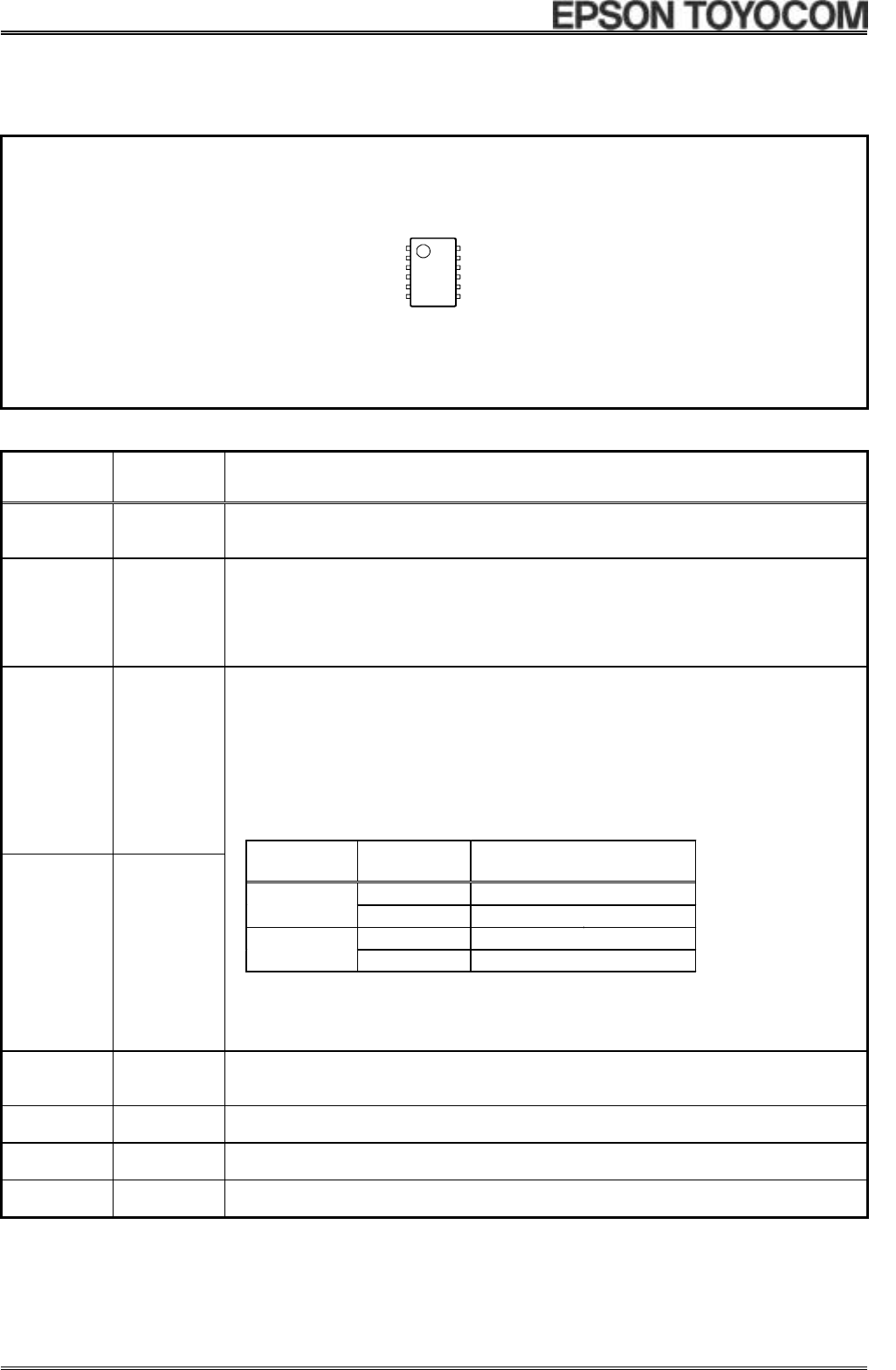
3. Terminal description
3.1. Terminal connections
RX
−
8564
LC
1.
N.C.
12.
N.C.
2.
N.C.
11. CLKOE
3.
N.C.
10. V
DD
4.
N.C.
9. CLKOUT
5. /INT 8. SCL
6. GND
#
1
# 6
#
12
# 7
7. SDA
VSOJ
−
12pin
3.2. Pin Functions
Signal
name
I/O Function
SCL Input This is the serial clock input pin for I
2
C Bus communications.
SDA Bi-Directional
This pin's signal is used for input and output of address, data, and ACK bits,
synchronized with the serial clock used for I
2
C communications.
Since the SDA pin is an N-ch open drain pin during output, be sure to connect a suitable
pull-up resistance relative to the signal line capacity.
CLKOUT Output
CLKOE Input
The CLKOUT pin is a clock output pin (C-MOS output) with the output control function.
The CLKOE pin can be used in combination with the FE bit, FD1 bit, and FD0 bit to
control the output mode of the CLKOUT output pin.
The CLKOE input pin can be used in combination with the FE bit, FD1 bit, and FD0 bit to
select the frequency output from the CLKOUT output pin (32.768 kHz, 1024 Hz, 32 Hz, or
1 Hz) or to stop output.
When output is stopped, the CLKOUT output pin is at low level ( = " L " ).
CLKOE pin
input
FE
bit
CLKOUT pin
output
1 Output
( C-MOS )
" H "
0
OFF
( " L " )
1
OFF
( " L " )
" L "
0
OFF
( " L " )
During the initial power-on (when power is applied from 0 V), if the CLKOE input pin is at
high level ( = " H " ), the power-on reset function selects 32.768 kHz as the frequency.
/INT Output
This pin outputs alarm signals, fixed timer interrupt signals, and other interrupt signals at
low level ( = " L " ). This pin is an open drain pin.
V
DD
−
This pin connects to the plus side of the power.
GND
−
This pin connects to the minus side (ground) of the power.
N.C.
−
This pin is not connected internally. Be sure to connect using OPEN, or GND or VDD.
Note : Be sure to connect a bypass capacitor rated at least 0.1 µF between V
DD
and GND.


