


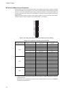

32
■ Setting the Memory Connective Switches
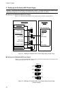
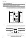
These switches can be used to disconnect address lines disabled by the memory capacity switching
function from buffers and using them as user resources instead when the external-memory emulation
function is used. Even when the external-memory emulation function is not used, the switches can
be used to disconnect those address lines from buffers to reduce the load on the address lines used as
user resources.
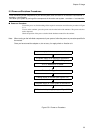
Figure 5.4-3 shows the factor settings of the switches; Table 5.4-2 lists the elements of the switches
and their respective signal conductors and evaluation MCU’s pin numbers.
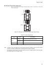
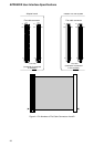
Figure 5.4-3 Setting the Memory Connective Switches (Factory Setting)
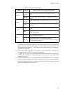
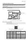
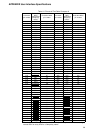
Table 5.4-2 The Memory Connective Switch Settings
* : The user resources corresponding to the above pin numbers are different depending on the eval-
uation MCU used.
For details, refer to the hardware manual for the evaluation MCU to be used or “APPENDIX
User Interface Specifications”.
Part number
(Printed on board)
Element number
(Labeled on switch)
Relevant signal
conductor
Evaluation MCU’s pin
number
SW2
1 P54 (RDX) 140
2 P21 (A1) 310
3 P22 (A2) 201
4 P23 (A3) 357
5 P24 (A4) 257
6 P25 (A5) 144
7 P26 (A6) 309
8 P27 (A7) 256
SW3
1 P30 (A8) 200
2 P31 (A9) 356
3 P32 (A10) 308
4 P33 (A11) 92
5 P34 (A12) 44
6 P35 (A13) 255
7 P36 (A14) 143
8 P37 (A15) 199
SW4
1 P40 (A16) 307
2 P41 (A17) 91
3 P42 (A18) 142
4 P43 (A19) 254
5 P44 (A20) 43
6 P45 (A21) 198
SW2
RD
A1
A2
A3
A4
A5
A6
A7
A16
A17
A18
A19
A20
A21
A8
A9
A10
A11
A12
A13
A14
A15
SW3
SW4
12345678
ON
12345678 12345678
ON
ON
Chapter 5 Usage