7
5. Setting of the Switch and Jumper Plug
■ Position of the switch and jumper plug
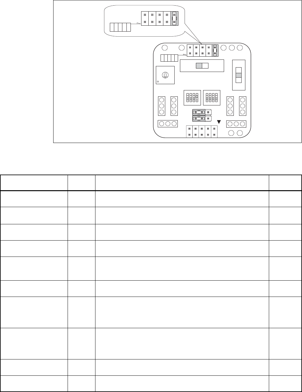
The positions of the switch and jumper plug on a MCU board is shown in Figure 8, and specifications
are shown in Table 3.
Figure 8 Positions of switches and jumper plugs on MCU board
Table 3 Switch and Jumper plug settings
Item
SW/S
name
Setting
Initial
setting
Clock selector switch (SW1-1)
ON : Disable the sub clock
OFF : Enable the sub clock
OFF
- (SW1-2)
For reserved bit,
Please set to OFF at all times.
OFF
APB8 bus output selector
switch
(SW1-3)
ON : Enable the APB8 bus
OFF : Disable the APB8 bus
OFF
C-pin selector switch (SW1-4)
ON : Connect the C pin and the on-board 0.1µF capacitor
OFF : Disconnect the C pin and the on-board 0.1µF capacitor
ON
Clock input selector
switch
(SW2)
Select the main clock and sub clock source on the MCU board or on
the user system. (See “■ Setting of clock input selector switch
(SW2)”.)
OFF
Product selector switch (SW3)
Set this switch depending on the number of pins on the target MCU
to be used. (See “■ Setting of the product selector switch (SW3)”.)
0
LVD selector switch (SW4)
Select the low-voltage detection function.
LVD1 : LVD1 enabled
OFF : LVD function disabled
LVD2 : LVD2 enabled
OFF
Voltage selector switch (SW5)
Select 5V or 3V supply on the operating voltage of the evaluation
MCU.
5V : 5V supply
3V : 3V supply
5V
Sub clock selector jump-
er plug
(S1)
Select whether to use the sub clock. See the relevant table. (See “■
Settings of the sub clock selector jumper plug (S1)”.)
Jumper of
B-C
LVD2 detection voltage
setting jumper plug
(S2)
Set the LVD2 detection voltage. (See “■ Settings of the LVD2 de-
tection voltage jumper plug (S2)”.)
LVD0
LVD4
LVD3
LVD2
LVD1
LVD0
BGM
ADAPTER
SUB CLOCK
C B A
1
2
CLK
CLK S.V.
APB8
C
X0
X1
X0A
X1A
7
6
5
4
3
2
1
0
F
E
D
C
B
A
9
8
PRODUCT SELECT
LVD4
LVD3
LVD2
LVD1
LVD0
GND
VCC
3V5V
LVD2OFFLVD1
MAIN CLOCK
1 2 3 4 1 2 3 4
ON ON
SW5
SW4
SW2
SW1
SW3
S2
S2
SC2
SC3
SC1SC4
SC6
SC5


