


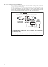
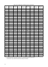
11
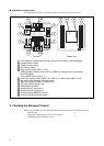
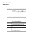
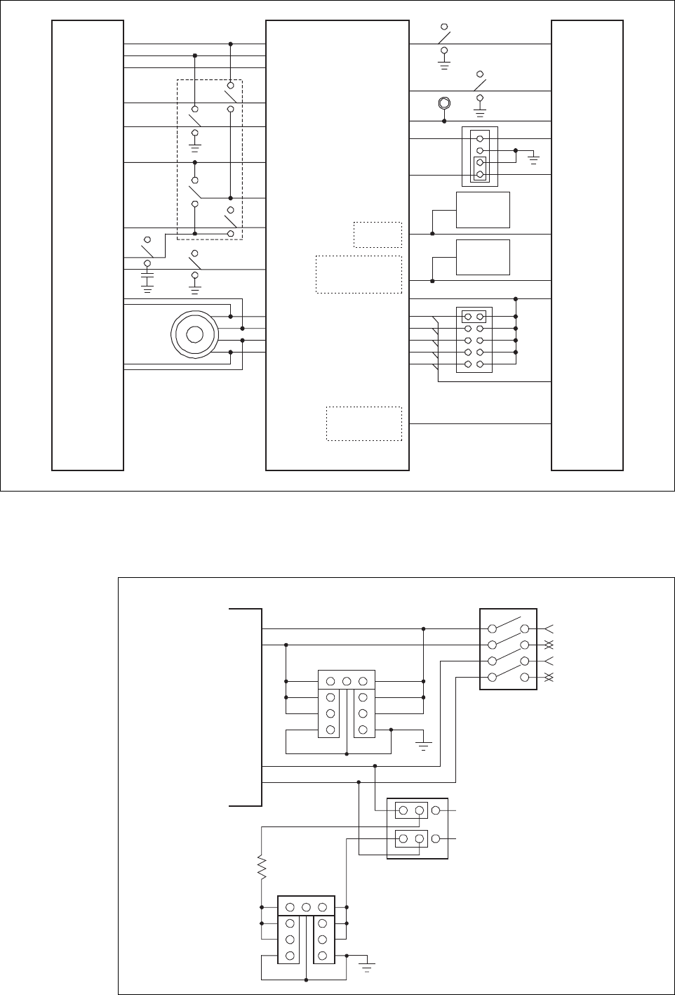
Figure 12 MCU board functional block diagram
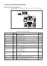
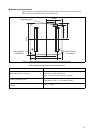
■ Clock settings
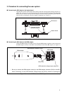
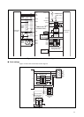
Figure 13 shows the clock-related circuit diagram.
Figure 13 Clock selector circuit
AVcc
AVR
AVss
AVcc3
AVR3
Vcc
C
PG0
SEL4
SEL0
SEL1
SEL2
SEL3
LVR0
LVR1
LVR2
LVR3
LVR4
LVDIN
X0,X1
X0A,X1A
LVDEN2
LVDEN
LVDREXT
APBEN
(Reserved)
Vcc,GND,BRSTX
BSIN,BSOUT
BDBMX,BEXCK
0
0
0
0
0
0
0
0
1
2
1
1
1
1
1
1
1
1
4
2
3
1
2
3
4
5
0
1
3
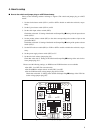
Header board
connector
Header board
connector
Voltage
selector
switch
C-pin
selector
switch
Product
selector
switch
Clock selector
switch
MB95FV100-103
(Evaluation MCU)
Other pins
LVD2 detection voltage
setting jumper plug
BGM
adapter
connector
Clock
selector
circuit
LVD
selector
switch
APB8 bus output
selector switch
X0
X1
X0A
X1A
X0
X1
X0A
X1A
CBA
2
1
( R1)
( M1)
1
2
3
4
GND
GND
T4
U2
R3
V1
Crystal oscillator mounting
socket(Main Clock)
Sub clock selector
jumper plug
(S1)
Clock input selector
switch(SW2)
Crystal oscillator
mounting socket
(Sub Clock)