EM78P809N
8-Bit Microcontroller
Product Specification (V1.0) 07.26.2005
• 27
(This specification is subject to change without further notice)
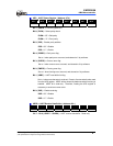
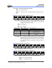
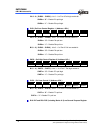
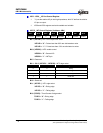
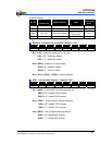
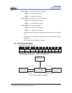
Bit 3 ( TBIE ) : Time base timer interrupt enable bit.
TBIE = “0” : disable TBIF interrupt
TBIE = “1” : enable TBIF interrupt
Bit 2 ( EXIE1 ) : External INT 1 Interrupt enable bit.
EXIE1 = “0” : disable EXIF1 interrupt
EXIE1 = “1” : enable EXIF1 interrupt
Bit 0 ( TCIE0 ) : TCC Interrupt enable bit.
TCIE0 = “0” : disable TCIF0 interrupt
TCIE0 = “1” : enable TCIF0 interrupt
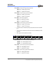
Individual interrupt is enabled by setting its associated control bit in the IMR2
to "1".
Global interrupt is enabled by the ENI instruction and is disabled by the DISI
instruction.
IMR2 register is both readable and writable.
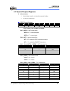
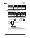
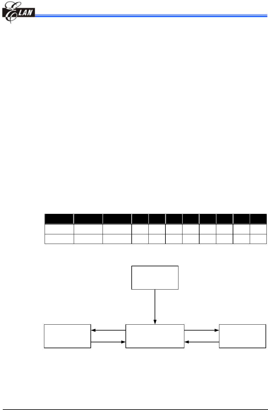
4.4 CPU Operation Mode
Registers for CPU operation mode
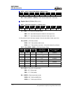
R_BANK Address NAME Bit 7 Bit 6 Bit 5 Bit 4 Bit 3 Bit 2 Bit 1 Bit 0
BANK 0 0X05 SCR 0 PS2 PS1 PS0 0 1 SIS REM
-- R/W R/W R/W -- -- R/W R/W
* R_BANK: Register Bank (bits 7, 6 of R3), R/W: Read/Write
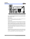
Reset Occurs
SIS=0 + SLEP
NORMAL MODE
CPU : Operating
Fosc: Oscillates
SLEEP MODE
CPU : Halts
Fosc: Stops
IDLE MODE
CPU : Halts
Fosc: Oscillates
Interrupt
SIS=1 + SLEP
/SLEEP Pin Input
Fig 5. Operation Mode and Switching


