


EM78P809N
8-Bit Microcontroller
Product Specification (V1.0) 07.26.2005
• 3
(This specification is subject to change without further notice)
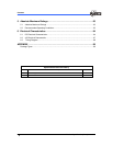
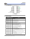
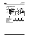
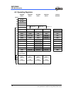
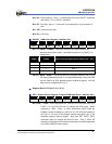
3 Pin Assignment
1
2
3
4
5
6
7
8
9
10
11
12
13
14 15
16
17
18
19
20
21
22
23
24
25
26
27
28
(ACLK) OSCO
OSCI
TEST
(AD0) P90
(AD1) P91
(AD2) P92
(AD3) P93
(AD4) P94
(AD5) P95
(AD6) P96
(AD7/VREF) P97
(TC3, INT3) P80
(TC4, /PWM, /PDO) P81
VSS
P70 (/SCK)
P71(RX,SI)
P72 (TX,SO)
P73 (/SLEEP, /INT5)
P60 (/INT0)
P61 (INT1)
P62 (TC2)
P63 (/TONE)
P64 (/SS)(OEB)
P65 (PGMB)
P66 (DATAIN)
P67 (DINCK)
/RESET (VPP)
VDD
EM78P809N
Fig. 1. Pin Assignment
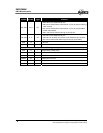
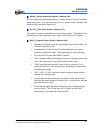
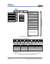
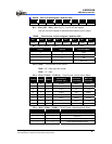
4 Pin Description
Table 1
Symbol Pin No. Type Function
VDD 28 - * Power supply
OSCI 2 I
* Crystal type: Crystal input terminal
* RC type: RC oscillator input pin
OSCO 1 I/O
* Crystal type: Output terminal for crystal oscillator
* RC type: Instruction clock output
* External clock signal input
/RESET 27 I
* Input pin with Schmitt trigger. If this pin remains at logic low, the
controller will also remain in reset condition.
P60~P67 19~26 I/O
* P60~P67 are bi-directional I/O pins
* P60 can be used as external interrupt 0 (/INT0)
* P61 can be used as external interrupt 1 (INT1)
* P62 can be used as 16-bit Timer/Counter 2 (TC2)
* P63 can be used as divider output (/TONE)
* P64 slave mode enable (/SS)
* P60 ~ P63 can be used as pull high or pull low pins
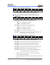
P70~P73 15~18 I/O
* P70~P77 are bi-directional I/O pins
* P70 can be used as SPI serial clock input/output (/SCK)
* P71 can be used as SPI serial data input (SI) or UART data receive
input (RX)
* P72 can be used as SPI serial data output (SO) or UART data
transmit output (TX)
* P73 can be used as SLEEP mode release input (/SLEEP) or external
interrupt input 5 (/INT5)
* P70 ~ P73 can be used as pull high or pull low pins