


User's Manual U13502EJ2V0UM00
91
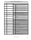
APPENDIX A NOTES ON DESIGNING A TARGET
Design a board using a flash microcontroller if you want to study the possibility of on-board writing.
•
Pin processing
The target may have pins that require special processing when the mode is changed from normal operating
mode to flash memory programming mode, or pins that go to high-impedance during programming. In a mode
in which the operation of the microcontroller is stopped by pin processing, the programming operation cannot be
performed. Therefore, be sure to read the manual for the device before creating the target.
•
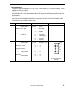
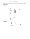
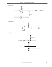
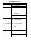
Interface circuit for the PG-FP3
Interface circuit examples for a UART (asynchronous communication port) and SIO (3-wire clocked port) are
given below. Because the PG-FP3 senses the voltage on the target even when V
DD
is not supplied to the target,
be sure to connect the V
DD
pin. For information on pin processing of the device, be sure to refer to the manual
for the device used.
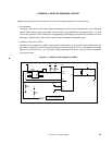
Figure A-1. Interface Circuit Example for a UART
V
CC
V
CC
JUMPER
User reset circuit
V
CC
V
CC
V
CC
R
10K
R
10K
R
10K
R
10K
CON
FAP-1008#2
Microcontroller
IC
Y
C
C
6
7
8
9
10
RESET
V
DD
V
PP
HS
NC
GND
SI
SO
SCK
CLK
1
2
3
4
5
TxD
X1
X2
RxD
V
PP
V
DD
V
SS
RESET