


©2002 Inova Computers GmbHPage 1-10 Doc. PD00581013.004
Product Overview
ICP-PIII
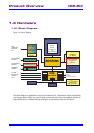
1.4 Hardware
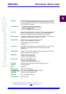
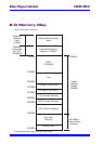
1.41 Block Diagram
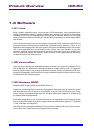
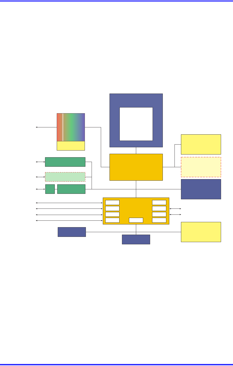
Figure 1.41 Block Diagram
This block diagram is applicable to all Inova’s PIII-based
CPUs. Components and/or functionality
may change without notice. An extra PCI load can be attached to the on-board 80-pin header. An
open specification is available allowing developers to manufacture their own PCI device.
USB
PS/2
COM 1/2
LPT 1 PCI2ISA Power
EIDE
FDC
IRQ
8/16 MByte
SGRAM
North Bridge
Intel 82443BX
RTC
128/384 MByte
Piggyback
Extension
SDRAM (ECC)
128 MByte
On-Board
ISA Bus
Floppy
Hard-Disk
(2 Channels. 4 Devices)
South
Bridge
ALi 1543C
10/100 Mbit/s
Ethernet
400 Mbit/s
FireWire
VGA
GigaST
Ȣ
R
PanelLink
TFT
2x USB
Mouse/Key.
COM1/2
LPT1
FLASH (BIOS)
PC100
AGP
PCI/PCI Bridge
System Slot
or
Peripheral Device
PCI Bus
TSB 12LV23
Intel 82559 Ethernet
Intel 82559 Ethernet
PL
Silicon Motion
Lynx3DM
or
ATI Radeon VE
Graphics
10/100 Mbit/s
Ethernet
Piggyback
Up to 512 MByte
M-Systems
Disk-On-Chip™
x86 ‘processor
Pentium III,
Celeron
Socket
FC-PGA 370
or
BGA2 (Mobile)