


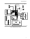

Motherboard Description
27
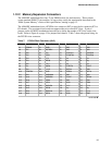
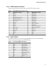
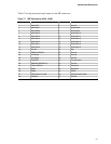
1.12.3 VESA Feature Connector
Table 8 provides the pinout and signal listing for the LBP VESA feature connector.
Table 8. LBP VESA Feature Connector (J1K1)
Pin Signal Name / Function
Pin
Signal Name / Function
1 Ground
2
Pixel Data 0
3 Ground
4
Pixel Data 1
5 Ground
6
Pixel Data 2
7 Enable External Pixel Data
8
Pixel Data 3
9 Enable External Sync
10
Pixel Data 4
11 Enable External Pixel Clock
12
Pixel Data 5
13 N/C, not used
14
Pixel Data 6
15 Ground
16
Pixel Data 7
17 Ground
18
PCLK, Pixel Clock
19 Ground
20
BLANKING
21 Ground
22
HSYNC, Horizontal Sync
23 N/C, not used
24
VSYNC, Vertical Sync
25 Key (no pin)
26
Ground
27 Key (no pin)
28
Key (no pin)
29 IICCLK
30
Ground
31 IICDAT
32
N/C
33 EN1
34
EN2
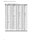
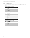
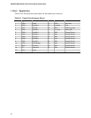
1.12.4 Serial Header
The COM2 serial port can be accessed using the COM2H header (J3N1) on the motherboard.
Table 9 lists the signals and pinout for the COM2H header.
Table 9. Serial Port (COM2H, J3N1) Pinout
Pin Signal Name Description
1 DCD Carrier Detect
2 DSR Data Set Ready
3 SIN# Serial Data In
4 RTS Request To Send
5 SOUT# Serial Data Out
6 CTS Clear To Send
7 DTR Data Terminal Ready
8 RI Ring Indicator
9 GND Chassis Ground
10 Key Vacant