Electrical Specifications
156 Intel® Xeon® Processor E5-1600/E5-2600/E5-4600 Product Families
Datasheet Volume One
7.1.9.2 Decoupling Guidelines
Due to its large number of transistors and high internal clock speeds, the processor is
capable of generating large current swings between low and full power states. This may
cause voltages on power planes to sag below their minimum values if bulk decoupling is
not adequate. Large electrolytic bulk capacitors (C
BULK
), help maintain the output
voltage during current transients, for example coming out of an idle condition. Care
must be taken in the baseboard design to ensure that the voltages provided to the
processor remain within the specifications listed in Table 7-11. Failure to do so can
result in timing violations or reduced lifetime of the processor. For further information,
refer to the appropriate Platform Design Guide (PDG).
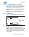
7.1.9.3 Voltage Identification (VID)
The Voltage Identification (VID) specification for the V
CC,
V
SA
, V
CCD
voltage are defined
by the
VR12/IMVP7 Pulse Width Modulation Specification. The reference voltage or the
VID setting is set via the SVID communication bus between the processor and the
voltage regulator controller chip. The VID settings are the nominal voltages to be
delivered to the processor's V
CC,
V
SA
, V
CCD
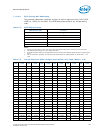
lands. Table 7-3 specifies the reference
voltage level corresponding to the VID value transmitted over serial VID. The VID codes
will change due to temperature and/or current load changes in order to minimize the
power and to maximize the performance of the part. The specifications are set so that a
voltage regulator can operate with all supported frequencies.
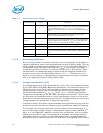
Individual processor VID values may be calibrated during manufacturing such that two
processor units with the same core frequency may have different default VID settings.
The processor uses voltage identification signals to support automatic selection of V
CC,
V
SA
, and V
CCD
power supply voltages. If the processor socket is empty (SKTOCC_N
high), or a “not supported” response is received from the SVID bus, then the voltage
regulation circuit cannot supply the voltage that is requested, the voltage regulator
must disable itself or not power on. Vout MAX register (30h) is programmed by the
processor to set the maximum supported VID code and if the programmed VID code is
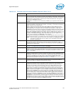
Table 7-1. Power and Ground Lands
Power and
Ground Lands
Number of
Lands
Comments
V
CC
208 Each V
CC
land must be supplied with the voltage determined by the
SVID Bus signals. Table 7-3 Defines the voltage level associated with
each core SVID pattern.Table 7-11, Figure 7-2, and Figure 7-5
represent V
CC
static and transient limits. VCC has a VBOOT setting of
0.0V.
V
CCPLL
3Each V
CCPLL
land is connected to a 1.80 V supply, power the Phase
Lock Loop (PLL) clock generation circuitry. An on-die PLL filter
solution is implemented within the processor.
V
CCD_01
V
CCD_23
51 Each V
CCD
land is connected to a switchable 1.50 V and 1.35 V supply,
provide power to the processor DDR3 interface. These supplies also
power the DDR3 memory subsystem. V
CCD
is also controlled by the
SVID Bus. V
CCD
is the generic term for V
CCD_01
, V
CCD_23
.
V
TTA
14 V
TTA
lands must be supplied by a fixed 1.05 V supply.
V
TTD
19 V
TTD
lands must be supplied by a fixed 1.05 V supply.
V
SA
25 Each V
SA
land must be supplied with the voltage determined by the
SVID Bus signals, typically set at 0.965V. VSA has a VBOOT setting of
0.9 V.
V
SS
548 Ground


