


UPI-C42UPI-L42
b Apply access code to appropriate inputs to put
the device into security mode
c Apply high voltage to EA and V
DD
pins
d Follow the programming procedure as per the
Quick-Pulse Programming Algorithm with known
data on the databus Not only the security bit but
also the security byte of the signature row is pro-
grammed
e Verify that the security byte of the signature
mode contains the same data as appeared on
the data bus (If DB0–DB7
e
high the security
byte will contain FFH)
f Read two consecutive known bytes from the
EPROM array and verify that the wrong data are
retrieved in at least one verification If the
EPROM can still be read the security bit may
have not been fully programmed though the se-
curity byte in the signature mode has
Verification
Since the security bit address overlaps the address
of the security byte of the signature mode it can be
used to check indirectly whether the security bit has
been programmed or not Therefore the security bit
verification is a mere read operation of the security
byte of the signature row (0FFH
e
security bit pro-
grammed 00H
e
security bit unprogrammed) Note
that during the security bit programming the reading
of the security byte does not necessarily indicate
that the security bit has been successfully pro-
grammed Thus it is recommended that two consec-
utive known bytes in the EPROM array be read and
the wrong data should be read at least once be-
cause it is highly improbable that random data coin-
cides with the correct ones twice
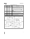
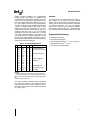
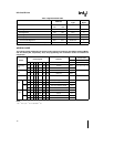
SIGNATURE MODE
The UPI-C42 has an additional 64 bytes of EPROM
available for Intel and user signatures and miscella-
neous purposes The 64 bytes are partitioned as fol-
lows
A Test codechecksumThis can accommodate
up to 25 bytes of code for testing the internal
nodes that are not testable by executing from the
external memory The test codechecksum is
present on ROMs and OTPs
B Intel signatureThis allows the programmer to
read from the UPI-41AH42AHC42 the manu-
facturer of the device and the exact product
name It facilitates automatic device identification
and will be present in the ROM and OTP ver-
sions Location 10H contains the manufacturer
code For Intel it is 89H Location 11H contains
the device code
The code is 43H and 42H for the 8042AH80C42
and OTP 8742AH87C42 respectively The
code is 44H for any device with the security bit
set by Intel
C User signatureThe user signature memory is
implemented in the EPROM and consists of 2
bytes for the customer to program his own signa-
ture code (for identification purposes and quick
sorting of previously programmed materials)
D Test signatureThis memory is used to store
testing information such as test data bin num-
ber etc (for use in quality and manufacturing
control)
E Security byteThis byte is used to check
whether the security bit has been programmed
(see the security bit section)
F UPI-C42 Intel SignatureApplies only to
CHMOS device Location 20H contains the man-
ufacturer code and location 21H contains the de-
vice code The Intel UPI-C42 manufacturer’s
code is 99H The device ID’s are 82H for the
OTP version and 83H for the ROM version The
device ID’s are the same for the UPI-L42
The signature mode can be accessed by setting
P10
e
0 P11–P17
e
1 and then following the pro-
gramming andor verification procedures The loca-
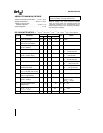
tion of the various address partitions are as shown in
Table 3
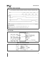
SYNC MODE
The Sync Mode is provided to ease the design of
multiple controller circuits by allowing the designer
to force the device into known phase and state time
The Sync Mode may also be utilized by automatic
test equipment (ATE) for quick easy and efficient
synchronizing between the tester and the DUT (de-
vice under test)
Sync Mode is enabled when SS
pin is raised to high
voltage level of
a
12 volts To begin synchroniza-
tion T0 is raised to 5 volts at least four clock cycles
after SS
T0 must be high for at least four X2 clock
cycles to fully reset the prescaler and time state
generators T0 may then be brought down during
low state of X2 Two clock cycles later with the ris-
ing edge of X2 the device enters into Time State 1
Phase 1 SS
is then brought down to 5 volts 4 clocks
later after T0 RESET is allowed to go high 5 tCY (75
clocks) later for normal execution of code
11