


UPI-C42UPI-L42
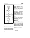
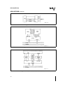
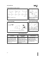
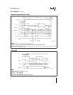
DRIVING FROM AN EXTERNAL SOURCE
290414–18
NOTE
See XTAL1 Configuration Table
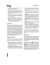
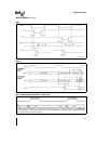
290414–19
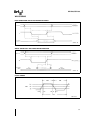
Rise and Fall Times Should Not
Exceed 10 ns Resistors to V
CC
are Needed to Ensure V
IH
e
35V
if TTL Circuitry is Used
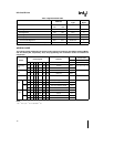
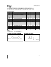
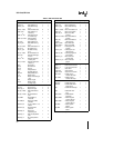
LC OSCILLATOR MODE
L C NOMINAL
f
e
1
2q
0
LC
45 H 20 pF 52 MHz
120 H 20 pF 32 MHz
C
e
C
a
3Cpp
2
Cpp
j
5–10pF
Pin-to-Pin Capacitance
290414–20
Each CShould beApproximately 20pF includingStray Capacitance
CRYSTAL OSCILLATOR MODE
290414–21
C1 5 pF (STRAY 5 pF)
C2 (CRYSTAL
a
STRAY) 8 pF
C3 20–30 pF INCLUDING STRAY
Crystal Series Resistance Should
be Less Than 30X at 125 MHz
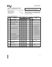
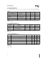
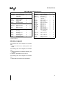
XTAL1 Configuration Table
XTAL1 Connection
1) to Ground
2) 10 KX Resistor
3) Not Connected
to Ground
Not recommended for CHMOS Recommended configuration for Low power configuration
designs Causes approximately designs which will use both recommended for CHMOS only
16 mA of additional current flow NMOS and CHMOS parts This designs to provide lowest
through the XTAL1 pin on UPI- configuration limits the additional possible power consumption
C42 and approximately 11 mA of current through the XTAL1 pin to This configuration will not work
additional current through XTAL1 approximately 1 mA while with the NMOS device
on the UPI-L42 maintaining compatibility with the
NMOS device
20