


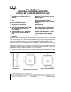
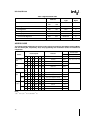

UPI-C42UPI-L42
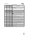
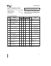
Table 1 Pin Description (Continued)
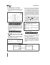
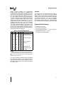
DIP PLCC QFP
Symbol Pin Pin Pin Type Name and Function
No No No
P
20
–P
27
21–24 24–27 39–42 IO PORT 2 8-bit PORT 2quasi-bidirectional IO lines The lower 4 bits
(P
20
–P
23
) interface directly to the 8243IO expander device and
35–38 39–42 11 13–15
contain address and data information duringPORT 4–7 accessP
21
can be programmed to provide hardwareA20 gate support The upper
4 bits (P
24
–P
27
) can be programmed to provideinterrupt Request and
DMA Handshake capability Software control canconfigure P
24
as
Output Buffer Full (OBF) interrupt P
25
as Input Buffer Full (IBF)
interrupt P
26
as DMA Request (DRQ) and P
27
as DMA ACKnowledge
(DACK
)
PROG 25 28 43 IO PROGRAM Multifunction pin used as theprogram pulse input during
PROM programming
During IO expander access the PROGpin acts as an addressdata
strobe to the 8243 This pinshould be tied high if unused
V
CC
40 44 17 POWER
a
5V main power supply pin
V
DD
26 29 1 POWER
a
5V during normal operation
a
1275V during programming
operation Low power standby supply pin
V
SS
20 22 38 GROUND Circuit ground potential
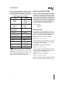
290414–4
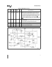
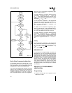
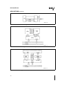
Figure 4 Block Diagram
3