


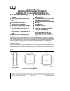
UPI-C42UPI-L42
UPI-42 COMPATIBLE FEATURES
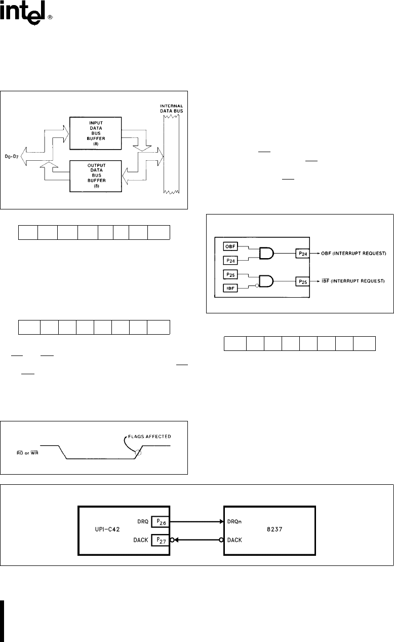
1 Two Data Bus Buffers one for input and one for
output This allows a much cleaner MasterSlave
protocol
290414–5
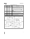
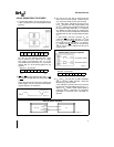
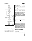
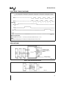
2 8 Bits of Status
ST
7
ST
6
ST
5
ST
4
F
1
F
0
IBF OBF
D
7
D
6
D
5
D
4
D
3
D
2
D
1
D
0
ST
4
–ST
7
are user definable status bits These
bits are defined by the ‘‘MOV STS A’’ single
byte single cycle instruction Bits 4–7 of the
acccumulator are moved to bits 4–7 of the status
register Bits 0–3 of the status register are not
affected
MOV STS A Op Code 90H
1 001000 0
D
7
D
0
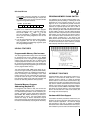
3 RD and WR are edge triggered IBF OBF F
1
and
INT change internally after the trailing edge of RD
or WR
During the time that the host CPU is reading the
status register the UPI is prevented from updat-
ing this register or is ‘locked out’
290414–6
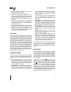
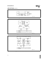
4 P
24
and P
25
are port pins or Buffer Flag pins
which can be used to interrupt a master proces-
sor These pins default to port pins on Reset
If the ‘‘EN FLAGS’’ instruction has been execut-
ed P
24
becomes the OBF (Output Buffer Full)
pin A ‘‘1’’ written to P
24
enables the OBF pin (the
pin outputs the OBF Status Bit) A ‘‘0’’ written to
P
24
disables the OBF pin (the pin remains low)
This pin can be used to indicate that valid data is
available from the UPI (in Output Data Bus Buff-
er)
If ‘‘EN FLAGS’’ has been executed P
25
be-
comes the IBF
(Input Buffer Full) pin A ‘‘1’’ writ-
ten to P
25
enables the IBF pin (the pin outputs
the inverse of the IBF Status Bit A ‘‘0’’ written to
P
25
disables the IBF pin (the pin remains low)
This pin can be used to indicate that the UPI is
ready for data
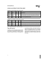
Data Bus Buffer Interrupt Capability
290414–7
EN FLAGS Op Code 0F5H
1 111010 1
D
7
D
0
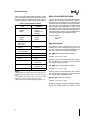
5 P
26
and P
27
are port pins or DMA handshake
pins for use with a DMA controller These pins
default to port pins on Reset
If the ‘‘EN DMA’’ instruction has been executed
P
26
becomes the DRQ (DMA Request) pin A ‘‘1’’
written to P
26
causes a DMA request (DRQ is
activated) DRQ is deactivated by DACK
RD
DACK
WR or execution of the ‘‘EN DMA’’ in-
struction
DMA Handshake Capability
290414–8
5