


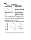
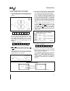
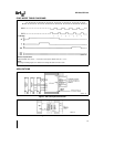

UPI-C42UPI-L42
This circuitry gives the host direct control of port 2
bit 1 (P21) without intervention by the internal CPU
When this opcode is executed P21 becomes a ded-
icated output pin The status of this pin is read-able
but can only be altered through a valid ‘‘D1’’ com-
mand sequence (see Table 1)
SUSPEND Invoke Suspend Power Down Mode
OPCODE 1000 0010 (82h) or 1110 0010
(E2h)
Enables device to enter micro power mode In this
mode the external oscillator is off CPU operation is
stopped and the Port pins are tristated This mode
can only be exited via a RESET signal
PROGRAMMING AND VERIFYING THE
UPI-C42
The UPI-C42 programming will differ from the NMOS
device in three ways First the C42 will have a 4K
user programmable array The UPI-C42 will also be
programmed using the Intel Quick-Pulse Program-
ming Algorithm Finally port 2 bit three (P23) will be
used during program as the extra address pin re-
quired to program the upper 2K bank of additional
memory None of these differences have any effect
on the full CHMOS to NMOS device compatibility
The extra memory is fully transparent to the user
who does not need or want to use the extra memo-
ry space of the UPI-C42
In brief the programming process consists of acti-
vating the program mode applying an address
latching the address applying data and applying a
programming pulse Each word is programmed com-
pletely before moving on to the next and is followed
by a verification step The following is a list of the
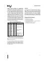
pins used for programming and a description of their
functions
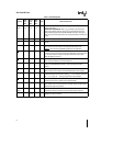
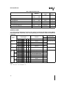
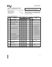
Pin Function
XTAL 2 Clock Input
Reset Initialization and Address Latching
Test 0 Selection of Program or Verify Mode
EA Activation of ProgramVerify Signature
RowSecurity Bit Modes
BUS Address and Data Input
Data Output During Verify
P
20–23
Address Input
V
DD
Programming Power Supply
PROG Program Pulse Input
WARNING
An attempt to program a missocketed UPI-C42 will result in
severe damage to the part An indication of a properly
socketed part is the appearance of the SYNC clock output
The lack of this clock may be used to disable the program-
mer
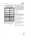
The ProgramVerify sequence is
1 Insert 87C42 in programming socket
2 CS
e
5V V
CC
e
5V V
DD
e
5V RESET
e
0V
A
0
e
0V TEST 0
e
5V clock applied or inter-
nal oscillator operating BUS floating PROG
e
5V
3 TEST 0
e
0V (select program mode)
4 EA
e
1275V (active program mode)
5 V
CC
e
625V (programming supply)
6 V
DD
e
1275V (programming power)
7 Address applied to BUS and P
20–23
8 RESET
e
5V (latch address)
9 Data applied to BUS
10 PROG
e
5V followed by one 100 ms pulse to
0V
11 TEST 0
e
5V (verify mode)
12 Read and verify data on BUS
13 TEST 0
e
0V
14 RESET
e
0V and repeat from step 6
15 Programmer should be at conditions of step 1
when the 87C42 is removed from socket
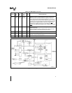
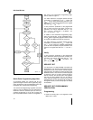
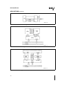
Please follow the Quick-Pulse Programming flow
chart for proper programming procedure shown in
Figure 6
9