


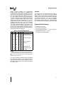
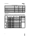
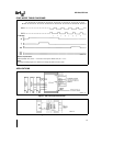
UPI-C42UPI-L42
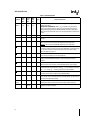
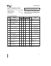
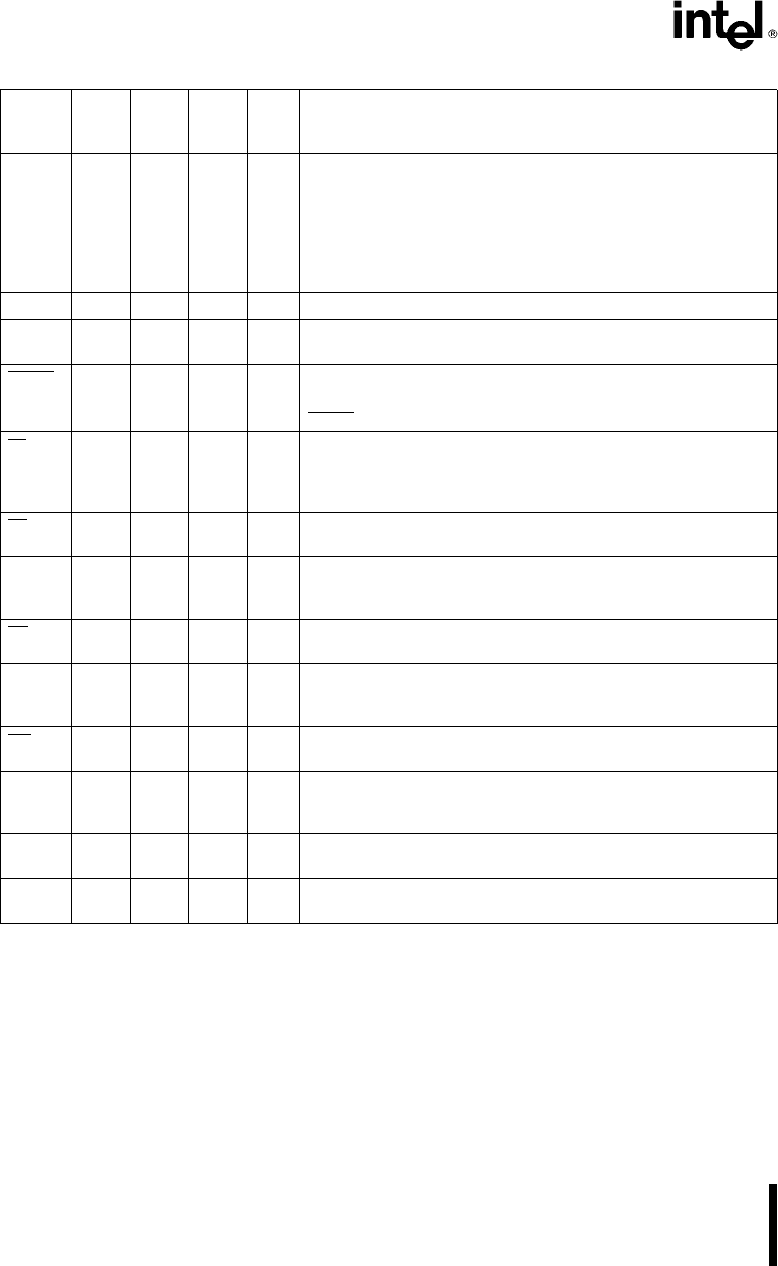
Table 1 Pin Description
DIP PLCC QFP
Symbol Pin Pin Pin Type Name and Function
No No No
TEST 0 1 2 18 I TEST INPUTS Input pins whichcan be directly tested using conditional
branch instructions
TEST 1 39 43 16
FREQUENCY REFERENCE TEST 1 (T
1
) functions as the event timer
input (under software control) TEST 0(T
0
) is a multi-function pin used
during PROM programming and ROMEPROM verification during Sync
Mode to reset the instruction stateto S1 and synchronize the internal clock
to PH1
XTAL 1 2 3 19 O OUTPUT Output from the oscillator amplifier
XTAL 2 3 4 20 I INPUT Input to theoscillator amplifier and internal clock generator
circuits
RESET 4 5 22 I RESET Inputused to reset status flip-flops set the programcounter to
zero and force the UPI-C42 fromthe suspend power down mode
RESET
is also used during EPROM programming and verification
SS 5 6 23 I SINGLE STEP Single step inputused in conjunction with the SYNC output
to step the program through eachinstruction (EPROM) This should be tied
to
a
5V when not used This pinis also used to put the device inSync
Mode by applying 125V to it
CS 6 7 24 I CHIP SELECTChip select input used to select one UPImicrocomputer
out of several connected to acommon data bus
EA 7 8 25 I EXTERNAL ACCESS External accessinput which allows emulation
testing and ROMEPROM verification This pin should betied low if
unused
RD 8 9 26 I READ IO read input which enablesthe master CPU to read data and
status words from the OUTPUT DATABUS BUFFER or status register
A
0
91027ICOMMANDDATA SELECT Address Input usedby the master processor
to indicate whether byte transfer isdata (A
0
e
0 F1 is reset) or command
(A
0
e
1 F1 is set) A
0
e
0 during program and verify operations
WR 10 11 28 I WRITE IOwrite input which enables the master CPU to writedata and
command words to the UPI INPUTDATA BUS BUFFER
SYNC 11 13 29 O OUTPUT CLOCK Outputsignal which occurs once per UPI instruction
cycle SYNC can be used asa strobe for external circuitry it is alsoused to
synchronize single step operation
D
0
–D
7
(BUS)
12–19 14–21 30–37 IO DATA BUS Three-state bidirectional DATABUS BUFFER lines used to
interface the UPI microcomputer to an8-bit master system data bus
P
10
–P
17
27–34 30–33 2–10 IO PORT 1 8-bit PORT 1quasi-bidirectional IO lines P
10
–P
17
access the
signature row and security bit
35–38
2