


Chapter 3 Signal Connections
© National Instruments Corporation 3-13 SCXI-1122 User Manual
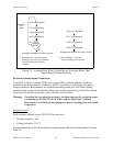
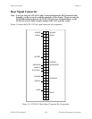
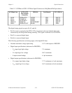
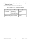
Table 3-2. SCXIbus to SCXI-1122 Rear Signal Connector to DAQ Board Pin Equivalences
SCXIbus Line SCXI-1122
Rear Signal
Connector
MIO-16 Lab Boards PC-LPM-16
MOSI SERDATIN ADIO0 PB4 DOUT4
D*/A DAQD*/A ADIO1 PB5 DOUT5
INTR* SLOT0SEL* ADIO2 PB6 DOUT6
SPICLK SERCLK EXTSTROBE* PB7 DOUT7
MISO SERDATOUT BDIO0 PC1 DIN6
The digital timing signals are pins 36, 43, and 46.
• Pin 36 is used as a clock by the SCXI-1122 to increment to the next channel after each
conversion by the DAQ board during scanning. This signal is referred to as SCANCLK.
• Pin 43 is a reserved digital input.
• Pin 46 is a reserved digital input.
The following specifications and ratings apply to the digital I/O lines:
• Absolute maximum voltage input rating 5.5 V with respect to DIGGND
• Digital input specifications (referenced to DIGGND):
-V
IH
input logic high voltage 2 V minimum
-V
IL
input logic low voltage 0.8 V maximum
-I
I
input current leakage ±1 µA maximum
• Digital output specifications (referenced to DIGGND):
-V
OH
output logic high voltage 3.7 V minimum at 4 mA maximum
-V
OL
output logic low voltage 0.4 V maximum at 4 mA maximum