


Table of Contents
© National Instruments Corporation vii VXIpc 800 Series User Manual
Index
Figures
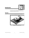
Figure 1-1. VXIpc-850 Embedded Computer ..........................................................1-1
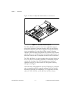
Figure 1-2. VXIpc-860 Embedded Computer ..........................................................1-2
Figure 2-1. VXIpc 800 Series Block Diagram .........................................................2-2
Figure 3-1. VXIpc 800 Series Parts Locator Diagram .............................................3-2
Figure 3-2. VXIbus Slot Configuration....................................................................3-5
Figure 3-3. VXIbus CLK10 Routing........................................................................3-6
Figure 3-4. SMB CLK10 Direction..........................................................................3-6
Figure 3-5. SMB CLK10 Termination .....................................................................3-7
Figure 3-6. SMB CLK10 Polarity ............................................................................3-7
Figure 3-7. SMB Trigger Input Termination............................................................3-8
Figure 3-8. Power-On Self Configuration Status .....................................................3-8
Figure 3-9. EEPROM Configuration........................................................................3-9
Figure 3-10. SCSI Termination ..................................................................................3-11
Figure 3-11. GPIB Interrupt Level .............................................................................3-11
Figure 3-12. System CMOS .......................................................................................3-12
Figure 3-13. Parallel Port DMA Channel...................................................................3-12
Figure 3-14. Ethernet Power-On Defaults..................................................................3-13
Figure D-1. VXIpc-800 Front Panel Layout and Dimensions ..................................D-2
Figure D-2. Keyboard and Mouse Connectors Location and Pinout ........................D-3
Figure D-3. VGA Connector Location and Pinout....................................................D-4
Figure D-4. Ethernet Connector Location and Pinout...............................................D-5
Figure D-5. COM1 and COM2 Connectors Location and Pinout.............................D-7
Figure D-6. Parallel Port Connector Location and Pinout ........................................D-8
Figure D-7. SCSI Connector Location and Pinout (SCSI II)....................................D-10
Figure D-8. GPIB Connector Location and Pinout ...................................................D-12
Figure D-9. SMB Connectors Location and Pinout ..................................................D-14
Figure D-10. Speaker Connection Location................................................................D-15
Figure D-11. VXIbus Connectors Location and Pinout..............................................D-17
Figure E-1. I/O Board Dimensions for VXIpc-850 Expansion Slot.........................E-1
Figure E-2. Component Height Restrictions for PCI Plug-In Boards Used with the VXIpc-850
E-2
Figure E-3. Length Restrictions for ISA Plug-In Boards Used with the
VXIpc-850 when SIMMs Taller than 0.85 in. are Used........................E-3
Figure E-4. I/O Board Dimensions for VXIpc-860 Expansion Slot.........................E-4