DDR3THIN-MN-XXX 73 Doc. Rev. 1.11
APPENDIX A – How DDR Data is Clocked
A.1 Background
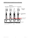
Demultiplexing means that the TLA’s Logic Analyzer card can have one data probe connected to
the target yet store incoming data in two or four separate data sections of the card. For instance,
the A3 data section (8-bits) can be connected to the target and data can be stored in the A3
section and the D3 section. Using the equivalent of 4X demux (by utilizing both the cross-point
switch and prime memory capabilities of the acquisition card), connections made to the A3
channels permit data to be stored in the A3, A3B (prime channels), D3 and D3B sections. A very
useful side benefit of using demux is that, since only one set of TLA data channels has to be
connected, only one probe load is added to the target, even though data is stored in two or four
different locations of the acquisition card.
A.2 DDR Acquisition - General
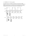
All of the above is background necessary to understand how the TLA is able to acquire data at
rates that initially look too fast. The speeds of DDR3 (1066 MT/s) require different setups to
enable proper data acquisition. In addition, instead of trying to use the 8 Data Strobes to acquire
data our solution uses CLK0 of the DDR SDRAM Clocks and all data acquisition is adjusted in
relation to the clock edges. The 8 Data Strobes cannot be easily used to acquire data as some
TLA configurations only support 4 Clock Inputs. Also, the Strobes cannot be used to acquire
Address and Command information.


