DDR3THIN-MN-XXX 75 Doc. Rev. 1.11
APPENDIX B - Considerations
B.1 NEX-DDR3INTR-THIN Bus Loading
It must be noted that the NEX-DDR3INTR-THIN Interposer is designed to minimal effect on the
user’s circuit. The acquired signals are sampled at top edge connector, and then passed through
isolation resistors to the probe. There will be an effective 600 ohm load on all probed signals.
The B_DDR3D_3A support will use two Interposers and will double probe all signal. Thus the
DC load will be near 300 ohms. The DDR3 Interposer has been tested via detailed simulations,
and by actual in circuit testing.
B.2 DIMM connector location for best quality signal capture
An interposer is subject to reflected noise and the quality of the acquisitions should improve if
the Interposer is in the furthest slot away from the memory controller. If the memory channel
contains two DIMM slots and only one will be used, the slot used must be the furthest away from
the memory controller.
B.3 TLA7BB4 Module to module skew
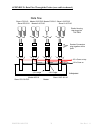
At print time Tektronix had not yet specified the module to module skew that will be displayed
in MagniVu, and timing modes. This skew is around 300ps. It is expected that in future releases
Tektronix will remove this skew. Contact Tektronix for updates.


