6.4. FACSIMILE SECTION
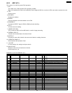
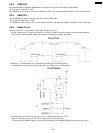
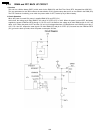
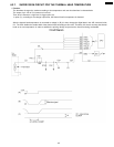
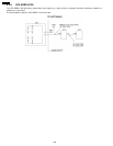
6.4.1. IMAGE DATA FLOW DURING FACSIMILE OPERATION
COPY (Fine, Super-Fine, Half Tone)
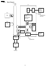
1. Line information is read by CIS, via route (1), and is input to IC1.
2. In IC1, the data is adjusted to a suitable level for A/D conversion in the Analog Signal Processing Section, and via route (2)
it is input to A/D conversion (8 bit). After finishing A/D conversion, the data is input to the Image Processing Section via route
(3). Then via routes (4) and (5), it is stored in RAM as shading data.
3. The draft´s information that is read by CIS is input to IC1 via route (1). After it is adjusted to a suitable level for A/D
conversion via route (2), the draft´s information is converted to A/D (8 bit), and it is input to the Image Processing Section.
The other side, the shading data which flows from RAM via routes (6) and (7), is input to the Image Processing Section.
After finishing the draft´s information image processing, white is regarded as "0" and black is regarded as "1".
Then via routes (4) and (5), they are stored in RAM.
4. The white/black data stored as above is input to the P/S converter via routes (6) and (8).
The white/black data converted to serial data in the P/S converter is input to the Thermal Head via route (9) and is printed
out on recording paper.
Note:
Standard: Reads 3.58 times/mm
Fine: Reads 7.7 times/mm
Super-Fine: Reads 15.4 times/mm
Transmission
1. Same processing as COPY items 1) - 3).
2. The data stored in RAM of IC1 is output from IC1 via routes (6) and (10), and is stored in the system bus.
Via route (11), it is stored in the communication buffer inside RAM (IC3).
3. While fetching data stored in the communication buffer synchronous with the modem, the CPU inputs data to the modem
along route (12) and (14).
In the analog front end IC (IC5) it is converted to serial analog data and forwarded over telephone lines via the NCU Section.
Reception
1. The serial analog image data is received over telephone lines and input to the analog front end IC (IC5) via the NCU section,
where it is demodulated to parallel digital data. The balance data is sent to the modem. Then the CPU stores the data in
the communication buffer of RAM (IC3) along route (11) and (15).
2. The data stored in RAM (IC3) is decoded by the CPU via route (12), and is stored in RAM by routes (13) and (5).
3. Same processing as COPY item 4).
109
KX-FT21RS


