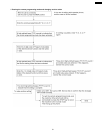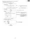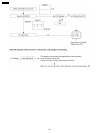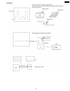
For these reasons and the software sequence to boot up the unit, if you use an oscilloscope to judge whether a signal is OK or NG,
you must check in the same order as in [List 1]. (If the ASIC (CPU) failed to access the ROM, the ASIC cannot access the SRAM
or DRAM normally.)
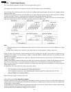
The digital circuit actually operates according to the timing combinations of these signals. So, if the timing of these signals is even
slightly off, the circuit will not operate normally. Even of the IC did malfunction, the output voltage level may become abnormal but
the timing is accurate according to the specifications. (If oscillation is provided accurately.)
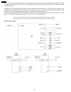
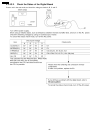
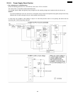
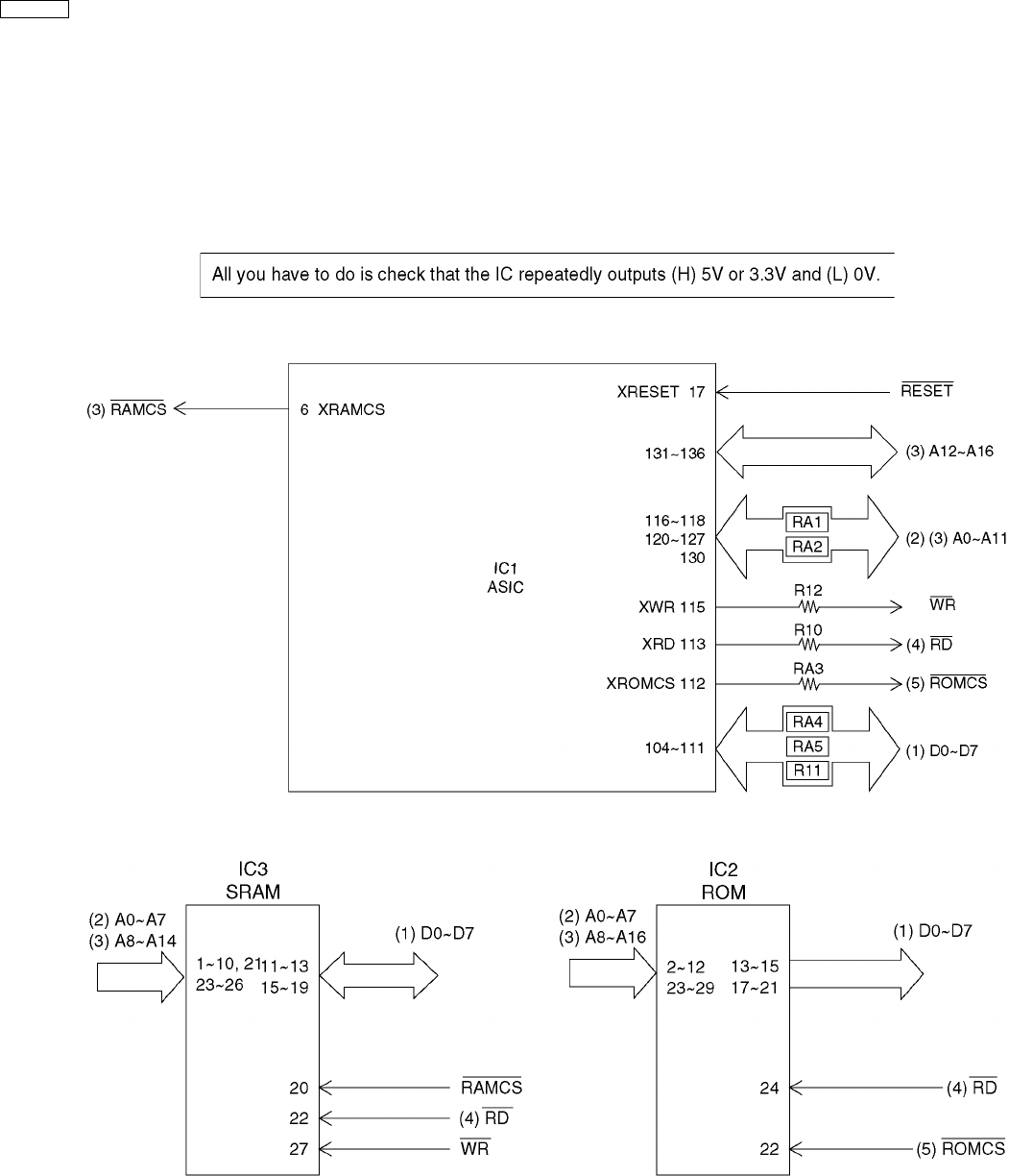
Accordingly, the problem presented here is whether each IC outputs the correct signal. (See the I/O and Pin No. diagram.) In other
words, is it constantly switching between 5V or 3.3V (H) and 0V (L) as described earlier.
I/O and Pin No. Diagram
58
KX-FT21RS


