


Philips Semiconductors ISP1301 USB OTG Transceiver Eval Kit User’s Guide
UM10028_1 © Koninklijke Philips Electronics N.V. 2003. All rights reserved.
User’s Guide Rev. 1.0—February 2003 12 of 18
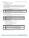
6. Hardware description
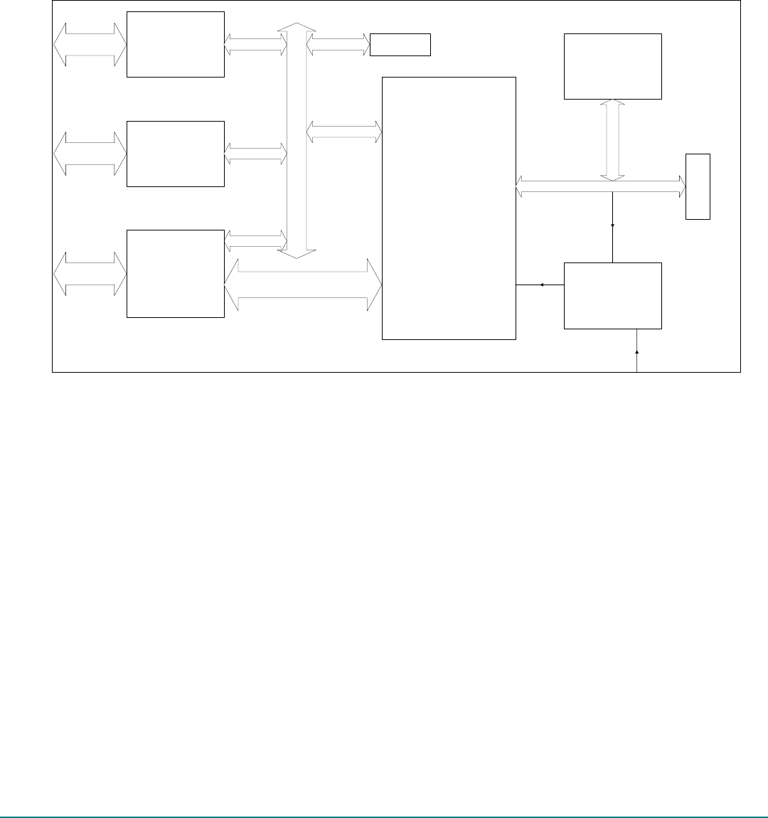
6.1. Block diagram
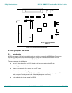
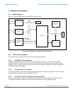
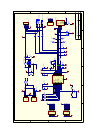
Figure 6-1 shows the block diagram of the ISP1301 evaluation board.
ISP1301
OTG TRANSCEIVER
AUDIO INTERFACE
(L/R SPEAKER LINE IN,
MIC PRE-AMP OUT)
PC PARALLEL-TO-I
2
C
CONVERTER
PCF8584 I
2
C-BUS
CONTROLLER
POWER MANAGER
ISA
PARALLEL
DP, DM, ID, V
BUS
I2C-BUS (SCL, SDA, ADR, INT)
DP, DM, ID
V
BUS
HC, DC and OTG CORE
LOGIC INTERFACE
CONNECTOR
(to the ISP1362 FPGA or
Phone FPGA)
CORE INTERFACE (OE, VP, VM, RCV,
SPEED, SUSPEND, RESET, V
DD_LGC
)
FPGA
INTERFACE
V
BAT
mini-AB Receptacle
V
ext
4-PIN I
2
C
HEADER
Figure 6-1: Block diagram of the ISP1301 evaluation board
6.2. Functional description
A brief description of each function module is given in the following sections.
6.2.1. PCF8584 I
2
C-bus controller
This block provides functions of the I
2
C-bus to the 8-bit parallel-bus converter. It can connect to the Philips
ISP1362 or ISP1161x ISA interface board, or any other generic 8-bit microprocessor interface through a 40-wire
IDE cable. The PC or other microprocessor can service the interrupt from the ISP1301 and access the registers of
the ISP1301 through this interface.
6.2.2. PC parallel to I
2
C converter
This interface provides an alternative method to access the ISP1301 I
2
C interface through the PC. The PC needs to
emulate software I
2
C master to access the ISP1301 I
2
C slave.
6.2.3. HC, DC and OTG core logic interface connector
This interface provides connection to a Host Controller (HC), Device Controller (DC) or On-The-Go (OTG)
core logic. This interface is used during OTG system-level evaluation or during compliance testing.