


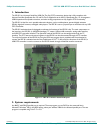
Philips Semiconductors ISP1301 USB OTG Transceiver Eval Kit User’s Guide
UM10028_1 © Koninklijke Philips Electronics N.V. 2003. All rights reserved.
User’s Guide Rev. 1.0—February 2003 6 of 18
3. Configurations and settings
3.1. Power requirements
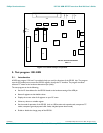
By default, the ISP1301 board is powered by a +5.0 V power supply through the DC jack (J12, inner +). The +5.0 V
power can also be supplied from the USB Type-B connector (J4). However, when J4 is connected to a USB port
on the PC, leave the USB mini-AB connector (J9) unconnected. If an external microprocessor is used to control
the I
2
C controller chip PCF8584 (U4), the +5.0 V power can also be supplied from pin 16 and pin 18 of the
microprocessor connector (J13).
When the +5.0 V power is correctly applied to the board, LED2 (green) will turn ON.
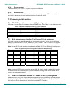
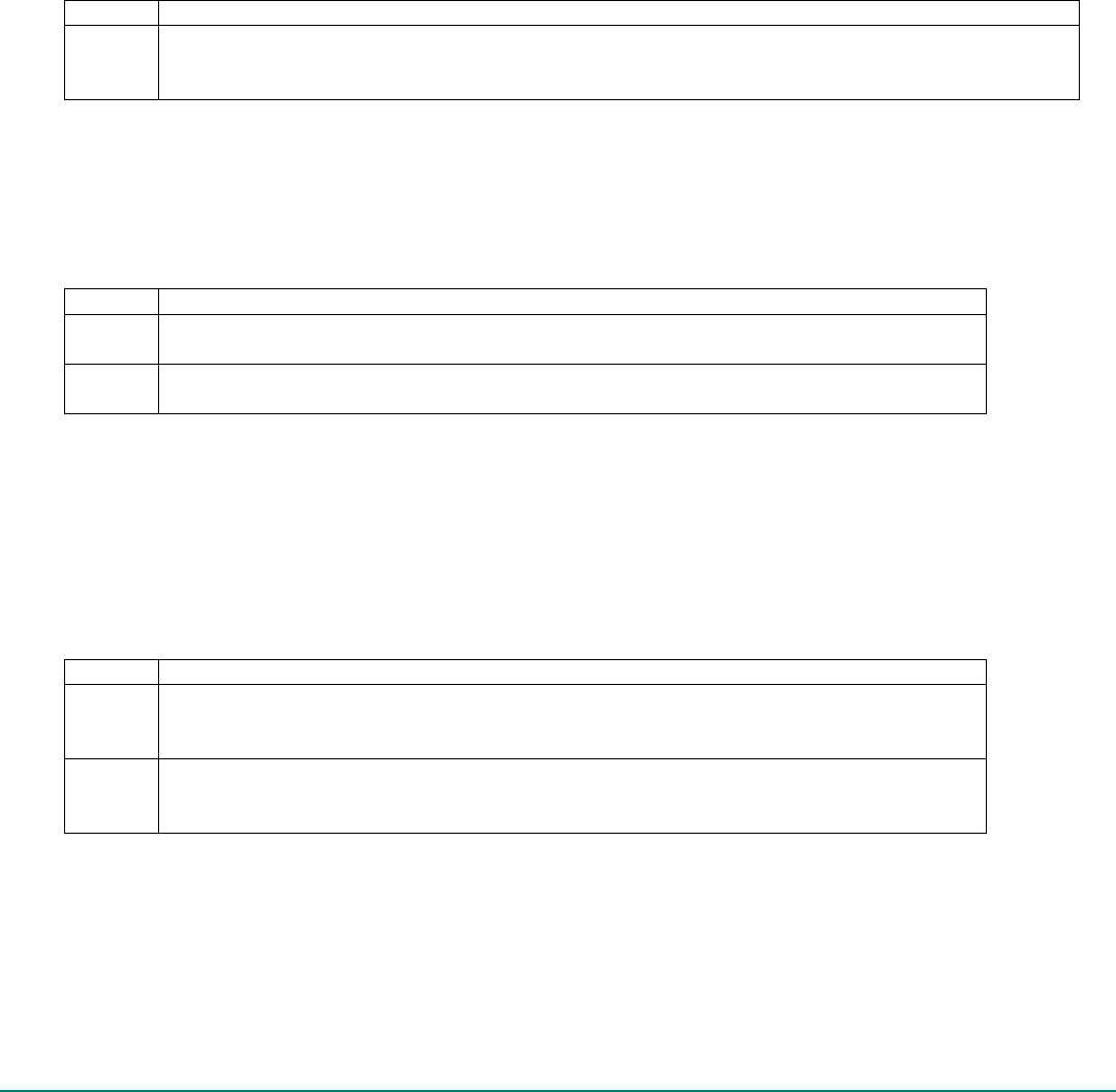
Table 3-1: +5.0 V power selection
Jumper Descriptions
JP6
Short 1(UP5V) and 2 (+5V): +5.0 V from the microprocessor interface (pin 16 or 18 of J13)
Short 3 (H_VBUS) and 4 (+5V): +5.0 V from the V
BUS
line of the USB connector (pin 1 of J4)
Short 5 (EXT5V) and 6 (+5V): +5.0 V from the DC jack (J12, inner +) [default]
The power supply (V
BAT
pin) for the ISP1301 can be provided either from the onboard +3.3 V source or from the
OTG Controller interface (pin 2 of J3).
Similarly, the power supply for the V
IO
(called V
DD_LGC
in the ISP1301 datasheet) pin of the ISP1301 can be provided
either from the onboard +3.3 V source or from the OTG Controller interface (pin 2 of J8).
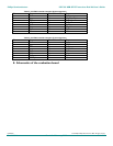
Table 3-2: V
BAT
and V
IO
selection
Jumper Descriptions
JP2
Short: V
BAT
from the onboard +3.3 V source [default]
Open: V
BAT
from the pin 2 of J3
JP5
Short: V
IO
from the onboard +3.3 V source [default]
Open: V
IO
from the pin 2 of J8
3.2. I
2
C master selection
The I
2
C master controller can be supplied from any one of three sources:
• PC parallel port (software I
2
C master)
• Philips I
2
C controller chip PCF8584 (hardware I
2
C master)
• External I
2
C master that is connected to the I
2
C header J11.
Table 3-3: I
2
C master selection
Jumper Descriptions
JP3
Short 1 (SDA_8584) and 2 (SDA5V): SDA from PCF8584
Short 2 (SDA5V) and 3 (SDA_PC): SDA from PC parallel port [default]
Open: SDA from I
2
C connector (pin 4 of J11)
JP4
Short 1 (SCL_8584) and 2 (SCL5V): SCL from PCF8584
Short 2 (SCL5V) and 3 (SCL_PC): SCL from PC parallel port [default]
Open: SCA from I
2
C connector (pin 3 of J11)
Note: SCL and SDA come from the same I
2
C master.