


Philips Semiconductors
User’s Manual - Preliminary -
P89LPC906/907/908
CLOCKS
2003 Dec 8 27
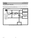
EXTERNAL CLOCK INPUT OPTION - P89LPC906
In this configuration, the processor clock is derived from an external source driving the XTAL1 / P3.1 pin. The rate may be from
0 Hz up to 12 MHz. The XTAL2 / P3.0 pin may be used as a standard port pin or a clock output.
.
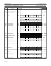
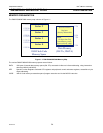
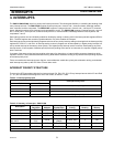
Figure 2-2: On-Chip RC Oscillator TRIM Register
CPU CLOCK (CCLK) WAKEUP DELAY
The P89LPC906/907/908 has an internal wakeup timer that delays the clock until it stabilizes depending to the clock source used.
If the clock source is any of the three crystal selections (P89LPC906), the delay is 992 OSCCLK cycles plus 60-100µs. If the
clock source is either the internal RC oscillator or the Watchdog oscillator, the delay is 224 OSCCLK cycles plus 60-100µs.
CPU CLOCK (CCLK) MODIFICATION: DIVM REGISTER
The OSCCLK frequency can be divided down, by an integer, up to 510 times by configuring a dividing register, DIVM, to provide
CCLK. This produces the CCLK frequency using the following formula:
CCLK frequency = f
OSC
/ (2N)
Where: f
OSC
is the frequency of OSCCLK
N is the value of DIVM.
Since N ranges from 0 to 255, the CCLK frequency can be in the range of f
OSC
to f
OSC
/510 ( for N =0, CCLK = f
OSC
) .
This feature makes it possible to temporarily run the CPU at a lower rate, reducing power consumption. By dividing the clock, the
CPU can retain the ability to respond to events other than those that can cause interrupts (i.e. events that allow exiting the Idle
mode) by executing its normal program at a lower rate. This can often result in lower power consumption than in Idle mode. This
can allow bypassing the oscillator start-up time in cases where Power down mode would otherwise be used. The value of DIVM
may be changed by the program at any time without interrupting code execution.
TRIM
Address: 96h
Not bit addressable
Reset Source(s): Power-up only
Reset Value: On power-up reset, ENCLK = 0, and TRIM.5-0 are loaded with the factory programmed value.
BIT SYMBOL FUNCTION
TRIM.7 - Reserved.
TRIM.6 ENCLK When ENCLK =1, CCLK/ 2 is output on the XTAL2 pin (P3.0) provided that the crystal
oscillator is not being used. When ENCLK=0, no clock output is enabled (P89LPC906).
TRIM.5-0 Trim value.
Note: on reset, the TRIM SFR is initialized with a factory preprogrammed value. When setting or clearing the ENCLK bit,
the user should retain the contents of bits 5:0 of the TRIM register. This can be done by reading the contents of the TRIM
register (into the ACC for example), modifying bit 6, and writing this result back into the TRIM register. Alternatively, the
"ANL direct" or "ORL direct" instructions can be used to clear or set bit 6 of the TRIM register.
76543210
- ENCLK TRIM.5 TRIM.4 TRIM.3 TRIM.2 TRIM.1 TRIM.0