


M3062PT2-EPB User’s Manual 4. Hardware Specifications
REJ10J0868-0200 Rev.2.00 January 16, 2006
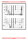
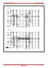
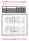
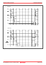
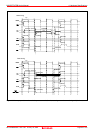
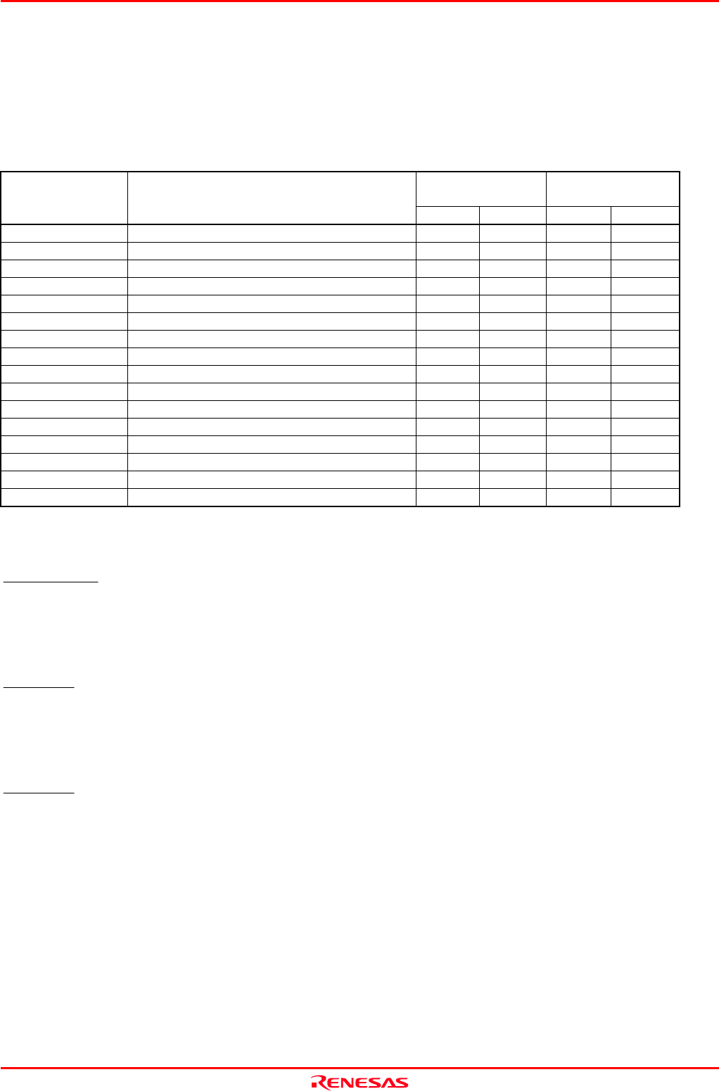
4.2.2 Operation Timing of Memory Expansion Mode and Microprocessor Mode (Vcc1=Vcc2=3V)
(1) Separate Bus Timing
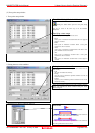
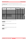
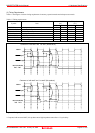
Table 4.5 and Figure 4.4 show the bus timing in memory expansion mode and microprocessor mode (3 wait, accessing external
area).
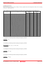
Table 4.5 Memory expansion mode and microprocessor mode (3 wait, accessing external area)
Actual MCU
[ns]
This product
[ns]
Symbol Item
Min. Max. Min. Max.
td(BCLK-AD) Address output delay time 30 See left
th(BCLK-AD) Address output hold time (BCLK standard) 4 See left
th(RD-AD) Address output hold time (RD standard) 0 -6
th(WR-AD) Address output hold time (WR standard) (*2) (*3)
td(BCLK-CS) Chip-select output delay time 30 See left
th(BCLK-CS) Chip-select output hold time (BCLK standard) 4 See left
td(BCLK-ALE) ALE signal output delay time 30 See left
th(BCLK-ALE) ALE signal output hold time -4 See left
td(BCLK-RD) RD signal output delay time 30 See left
th(BCLK-RD) RD signal output hold time 0 See left
td(BCLK-WR) WR signal output delay time 30 See left
th(BCLK-WR) WR signal output hold time 0 See left
td(BCLK-DB) Data output delay time (BCLK standard) 40 See left
th(BCLK-DB) Data output hold time (BCLK standard) 4 See left
td(DB-WR) Data output delay time (WR standard) (*1) See left
th(WR-DB) Data output hold time (WR standard) (*2) (*3)
*1 Calculated by the following formula according to the frequency of BCLK.
()
40
)(
105.0
9
−
×−
BCLKf
n
[ns] n: "3" for 3 wait
*2 Calculated by the following formula according to the frequency of BCLK.
)(
105.0
9
BCLKf
×
[ns]
*3 Calculated by the following formula according to the frequency of BCLK.
10
)(
105.0
9
−
×
BCLKf
[ns]
Page 77 of 102