


( 15 / 76 )
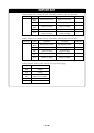
Note on Protect Resistor (PRC2):
•Make note of the fact that the protect is not canceled when protect register (PRC2), which enables
writing in the port P9 direction registers and the SI/O3, SI/O4 control registers, is changed with the
following procedure.
(1) Step execution of the instruction for setting ("1") PRC2
(2) Setting the break point from the instruction for setting ("1") PRC2 to when the setting the
register for the protect"
(3) Setting ("1") PRC2 from the dump window or script window
IMPORTANT
Note on Commands that Access the Single-step Interrupt Vector Area:
• Do not perform the following debugging operations with the single step interrupt vector area
(addresses FFFECh - FFFEFh).
(1) Step execution of instructions that access the single step interrupt vector area
(2) Program execution using instructions that access the single step interrupt vector area when a
software breakpoint is set in those instructions
Notes on Software Breaks and Hardware Breaks:
• Software breaks generate BRK interrupts by substituting the proper instruction to the BRK
instruction. Therefore, when referencing the result of a trace in bus mode, "00h" is displayed for
the instruction fetch address where a software break is set, and when referencing in reverse
assemble mode, "BRK" instruction is displayed.
• It is not possible to use a software break and a hardware break at the same time. If doing so, it may
not operate normally.
• In the area where the MAP setting is EXTERNAL, software breaks cannot be used.
Note on DMA Transfer:
•With this product, the program is stopped with a loop program to a specific address. Therefore, if
a DMA request is generated by a timer or other source while the program is stopped, DMA transfer
is executed. However, make note of the fact that DMA transfer while the program is stopped may
not be performed correctly. Also note that the following registers have been changed to generate
DMA transfer as explained here even when the program is stopped.
DMA0 transfer counter register: TCR0
DMA1 transfer counter register: TCR1