


( 60 / 76 )
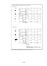
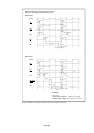
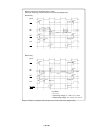
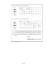
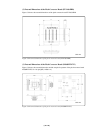
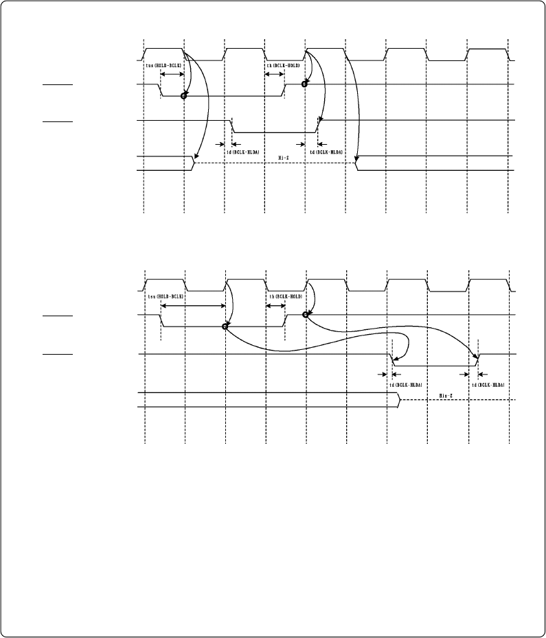
Figure 5.5 Timing requirements
Common to "with wait" and "no-wait" (actual MCU)
BCLK
P0, P1, P2,
P3, P4,
P50 to P52
Common to "with wait" and "no-wait" (This product)
BCLK
P0, P1, P2,
P3, P4,
P50 to P52
Note 1. Ports P00 to P52 will be high-impedance status regardless of the input level of BYTE pin
and ports P40 to P43 function selection bit (PM06) of the processor mode register 0.
Note 2. This product will be high-impedance status delaying by 2.5 cycles than an actual MCU.
Note 3. The setup time of HOLD is defined by the startup of BCLK, differently from that of actual
MCUs.
Conditions:
• V
CC = 5 V
• Input timing voltage: VIL = 1.0 V, VIH = 4.0 V
• Output timing voltage: VOL = 2.5 V, VOH = 2.5 V
HLDA output
HOLD input
HLDA output
HOLD input