


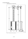
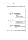
( 59 / 74 )
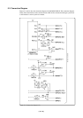
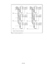
5.3 Operation Timing in Memory Expansion Mode and Microprocessor Mode
As there are a flexible cable and other devices between this product and the target system, I/O timing
will differ from that of the actual MCU. Use the following as a reference when using the emulation pod.
(1) The output signal (address, RD*, WR*, etc.) of the evaluation MCU mounted on this product
is output delayed by about 4 ns.
(2) It takes longer time to setup the data than actual MCU by approx. 8 ns.
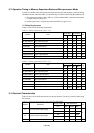
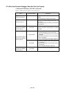
(1) Timing Requirements
Tables 5.2 and 5.3 list the timing requirements.
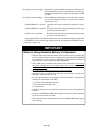
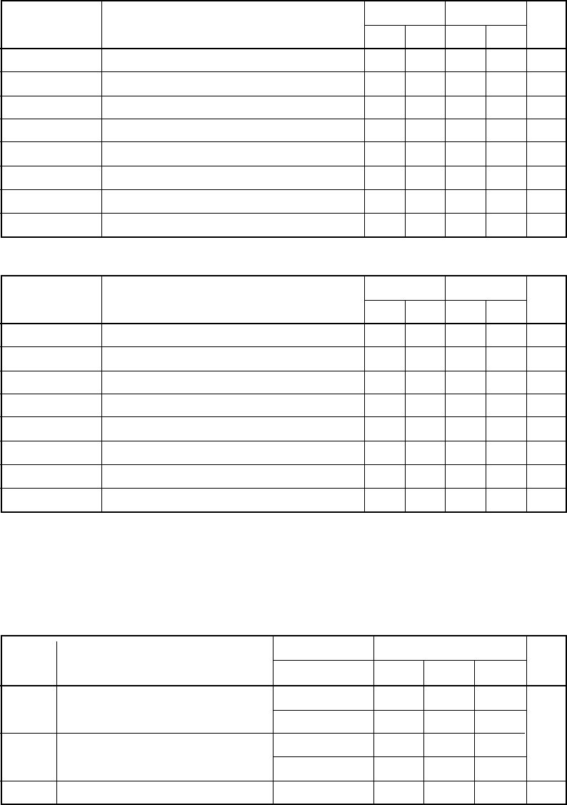
Table 5.2 Timing requirements (VCC = 5 V)
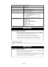
Table 5.3 Timing requirements (VCC = 3 V)
tsu (DB-BCLK)
tsu (RDY-BCLK)
tsu (HOLD-BCLK)
th (RD-DB)
th (CAS-DB)
th (BCLK-RDY)
th (BCLK-HOLD)
td (BCLK-HLDA)
Data input setup time
RDY* input setup time
HOLD* input setup time
Data input hold time
Data input hold time
RDY* input hold time
HOLD* input hold time
HLDA* output delay time
Min.
26
26
30
0
0
0
0
Max.
25
Min.
34
34
38
0
0
0
0
Max.
25
Actual MCU This product
Symbol
Item
Unit
ns
ns
ns
ns
ns
ns
ns
ns
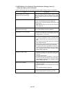
tsu (DB-BCLK)
tsu (RDY-BCLK)
tsu (HOLD-BCLK)
th (RD-DB)
th (CAS-DB)
th (BCLK-RDY)
th (BCLK-HOLD)
td (BCLK-HLDA)
Data input setup time
RDY* input setup time
HOLD* input setup time
Data input hold time
Data input hold time
RDY* input hold time
HOLD* input hold time
HLDA* output delay time
Min.
40
60
80
0
0
0
0
Max.
100
Min.
48
68
88
0
0
0
0
Max.
100
Actual MCU This product
Symbol
Item
Unit
ns
ns
ns
ns
ns
ns
ns
ns
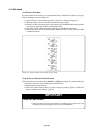
5.4 Electrical Characteristics
Table 5.4 shows IC electrical characteristics of the user interface. Use this as a reference when using
the emulator.
Table 5.4 Electrical characteristics of port P10 (TC74HC4066)
Symbol Parameter
Vcc
2.0
4.5
2.0
4.5
12.0
Max.
-
-
0.50
1.35
±100
Standard values
nA
Standard
-
-
-
-
-
V
IHC
VILC
Min.
1.50
3.15
-
-
-
High level control input voltage
Low level control input voltage
Measuring condition
Unit
V
Input currentIIN