


- 18 -
datasheet DDR3L SDRAM
Rev. 1.0
Unbuffered DIMM
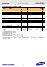
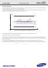
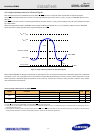
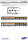
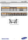
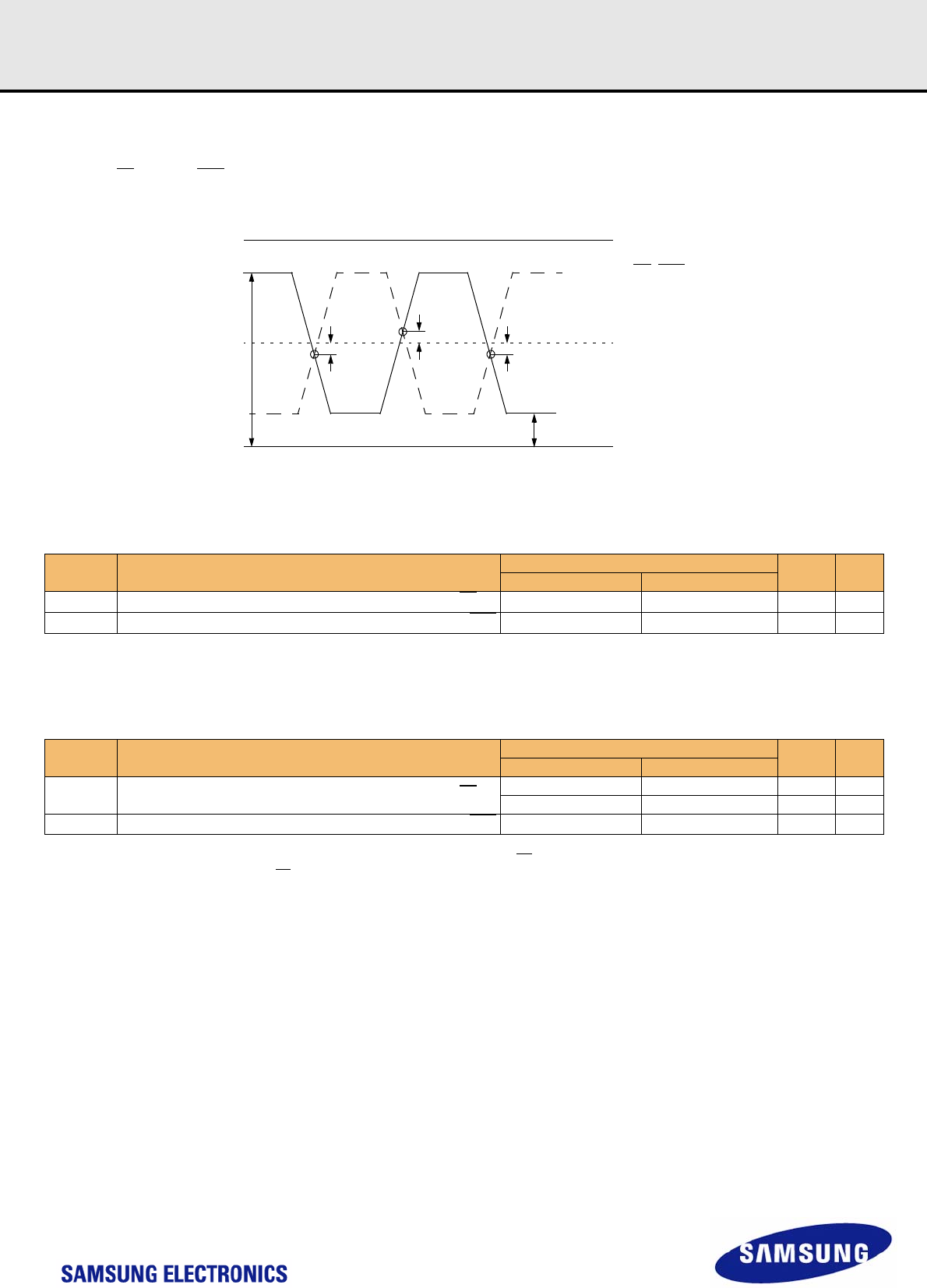
11.3.4 Differential Input Cross Point Voltage
To guarantee tight setup and hold times as well as output skew parameters with respect to clock and strobe, each cross point voltage of differential input
signals (CK, CK
and DQS, DQS) must meet the requirements in below table. The differential input cross point voltage V
IX
is measured from the actual
cross point of true and complement signal to the mid level between of V
DD
and V
SS
.
Figure 5. V
IX
Definition
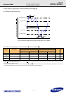
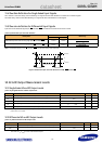
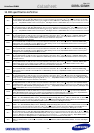
[ Table 7 ] Cross point voltage for differential input signals (CK, DQS) : 1.35V
NOTE :
1. The relationbetween Vix Min/Max and VSEL/VSEH should satisfy following.
(VDD/2) + Vix(Min) - VSEL ≥ 25mV
VSEH - ((VDD/2) + Vix(Max)) ≥ 25mV
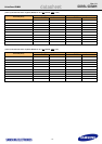
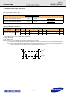
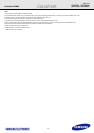
[ Table 8 ] Cross point voltage for differential input signals (CK, DQS) : 1.5V
NOTE :
1. Extended range for V
IX
is only allowed for clock and if single-ended clock input signals CK and CK are monotonic, have a single-ended swing V
SEL
/ V
SEH
of at least V
DD
/2
±250 mV, and the differential slew rate of CK-CK
is larger than 3 V/ ns.
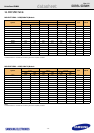
Symbol Parameter
DDR3L-800/1066/1333/1600
Unit NOTE
Min Max
V
IX
Differential Input Cross Point Voltage relative to V
DD
/2 for CK,CK
-150 150 mV 1
V
IX
Differential Input Cross Point Voltage relative to V
DD
/2 for DQS,DQS
-150 150 mV
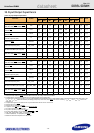
Symbol Parameter
DDR3-800/1066/1333/1600
Unit NOTE
Min Max
V
IX
Differential Input Cross Point Voltage relative to V
DD
/2 for CK,CK
-150 150 mV
-175 175 mV 1
V
IX
Differential Input Cross Point Voltage relative to V
DD
/2 for DQS,DQS
-150 150 mV
V
DD
CK, DQS
V
DD
/2
CK, DQS
V
SS
V
IX
V
IX
V
IX
VSEH VSEL