


- 33 -
datasheet DDR3L SDRAM
Rev. 1.0
Unbuffered DIMM
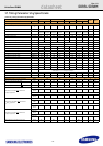
17.1 Jitter Notes
Specific Note a Unit ’tCK(avg)’ represents the actual tCK(avg) of the input clock under operation. Unit ’nCK’ represents one clock cycle of the
input clock, counting the actual clock edges.ex) tMRD = 4 [nCK] means; if one Mode Register Set command is registered at Tm,
another Mode Register Set command may be registered at Tm+4, even if (Tm+4 - Tm) is 4 x tCK(avg) + tERR(4per),min.
Specific Note b These parameters are measured from a command/address signal (CKE, CS
, RAS, CAS, WE, ODT, BA0, A0, A1, etc.) transition
edge to its respective clock signal (CK/CK
) crossing. The spec values are not affected by the amount of clock jitter applied (i.e.
tJIT(per), tJIT(cc), etc.), as the setup and hold are relative to the clock signal crossing that latches the command/address. That is,
these parameters should be met whether clock jitter is present or not.
Specific Note c These parameters are measured from a data strobe signal (DQS, DQS
) crossing to its respective clock signal (CK, CK) crossing.
The spec values are not affected by the amount of clock jitter applied (i.e. tJIT(per), tJIT(cc), etc.), as these are relative to the
clock signal crossing. That is, these parameters should be met whether clock jitter is present or not.
Specific Note d These parameters are measured from a data signal (DM, DQ0, DQ1, etc.) transition edge to its respective data strobe signal
(DQS, DQS
) crossing.
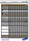
Specific Note e For these parameters, the DDR3 SDRAM device supports tnPARAM [nCK] = RU{ tPARAM [ns] / tCK(avg) [ns] }, which is in clock
cycles, assuming all input clock jitter specifications are satisfied. For example, the device will support tnRP = RU{tRP / tCK(avg)},
which is in clock cycles, if all input clock jitter specifications are met. This means: For DDR3-800 6-6-6, of which tRP = 15ns, the
device will support tnRP = RU{tRP / tCK(avg)} = 6, as long as the input clock jitter specifications are met, i.e. Precharge com-
mand at Tm and Active command at Tm+6 is valid even if (Tm+6 - Tm) is less than 15ns due to input clock jitter.
Specific Note f When the device is operated with input clock jitter, this parameter needs to be derated by the actual tERR(mper),act of the input
clock, where 2 <= m <= 12. (output deratings are relative to the SDRAM input clock.)
For example, if the measured jitter into a DDR3-800 SDRAM has tERR(mper),act,min = - 172 ps and tERR(mper),act,max = +
193 ps, then tDQSCK,min(derated) = tDQSCK,min - tERR(mper),act,max = - 400 ps - 193 ps = - 593 ps and tDQSCK,max(der-
ated) = tDQSCK,max - tERR(mper),act,min = 400 ps + 172 ps = + 572 ps. Similarly, tLZ(DQ) for DDR3-800 derates to
tLZ(DQ),min(derated) = - 800 ps - 193 ps = - 993 ps and tLZ(DQ),max(derated) = 400 ps + 172 ps = + 572 ps. (Caution on the
min/max usage!)
Note that tERR(mper),act,min is the minimum measured value of tERR(nper) where 2 <= n <= 12,
and tERR(mper),act,max is the maximum measured value of tERR(nper) where 2 <= n <= 12.
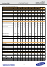
Specific Note g When the device is operated with input clock jitter, this parameter needs to be derated by the actual tJIT(per),act of the input
clock. (output deratings are relative to the SDRAM input clock.) For example, if the measured jitter into a DDR3-800 SDRAM has
tCK(avg),act = 2500 ps, tJIT(per),act,min = - 72 ps and tJIT(per),act,max = + 93 ps, then tRPRE,min(derated) = tRPRE,min +
tJIT(per),act,min = 0.9 x tCK(avg),act + tJIT(per),act,min = 0.9 x 2500 ps - 72 ps = + 2178 ps. Similarly, tQH,min(derated) =
tQH,min + tJIT(per),act,min = 0.38 x tCK(avg),act + tJIT(per),act,min = 0.38 x 2500 ps - 72 ps = + 878 ps. (Caution on the min/
max usage!)