


AN93
Rev. 1.3 111
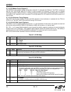
5.7.18. U6C (Line-Voltage Status Register)
U6C contains the line voltage status register, LVS, and resets to 0xXX00. Bits 7:0 are reserved, and a read returns
zero.
5.7.19. U6E–U7D (Modem Control and Interface Registers)
Modem Control and Interface registers include registers U6E, U70–U71, and U76–U79. These are bit-mapped
registers that control functions including TX/RX gain, clocking, I/O, SSI codecs, intrusion detection, and LVCS (line
voltage current sense).
U6E controls the clockout divider. Bits 15:13 and 7:0 are reserved. U6E resets to 0x1FA0 with a power-on or
manual reset (see Table 71).
Bits[12:8] (R1) control the R1 clockout divider. A 196.608 MHz clock signal passes through a divide-by (R
1
+1)
circuit to derive the CLKOUT signal. If R1 = 00000, CLKOUT is disabled. R1 is set at a default value of 11111,
which results in CLKOUT = 2.048 MHz. The CLKOUT adjustment range (15 <
R1 < 30) is 12.288 MHz to
6.342194 MHz.
U6F contains the parallel/SPI port receive FIFO interrupt timer and resets to 0x00FF.
Bits [15:8] are reserved and should not be written to any value other than 0.
Bits[7:0] set the period of an internal timer that is reset whenever the parallel or SPI port receive FIFO (Hardware
Interface Register 0) is read. If the internal timer expires with data in the receive FIFO, an interrupt is generated
regardless of the state of RXF (Hardware Interface Register 1 bit 7). This ensures that the host always removes all
receive data from the parallel or SPI port receive FIFO even if RXF is not set.
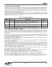
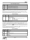
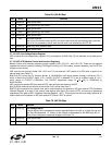
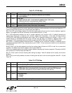
Table 69. U6A Bit Map*
Bit Name Function
15 Reserved Read returns zero.
14 SQ1 Spark quenching. See OHS2.
13 Reserved Read returns zero.
12 SQ0 Spark quenching. See OHS2.
11:3 Reserved Read returns zero.
2 OVL Overload Detected.
This bit has the same function as ROV, but clears itself after the overload has been removed.
This bit is only masked by the off-hook counter and is not affected by the BTE bit.
1 Reserved Read only; value indeterminate.
0 Reserved Read returns zero.
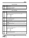
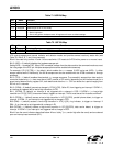
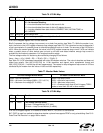
Table 70. U6C Bit Map
Bit Name Function
15:8 LVS[7:0] Line Voltage Status.
Eight-bit signed, two’s complement number representing the on-hook or off-hook tip-ring volt-
age. Each bit represents 1 V. Polarity of the voltage is represented by the MSB (sign bit). A
value of zero indicates a measured voltage of less than 3 V.
7:3 Reserved Read returns zero.
2:0 RXG[2:0] Global Receive Gain in dB (Default = 000b).