


AN93
26 Rev. 1.3
Bit 6 (TXE) is a read/write bit that gives the status of the 14-byte deep transmit FIFO. If TXE = 0, the transmit FIFO
contains three or more bytes. If TXE = 1, the transmit FIFO contains two or fewer bytes. Writing TXE = 0 clears the
interrupt but does not change the state of TXE.
Bit 5 (REM) is a read-only bit that indicates when the receive FIFO is empty. If REM = 0, the receive FIFO contains
valid data. If REM = 1, the receive FIFO is empty. The timer interrupt set by U6F ensures that the receive FIFO
contents 9 bytes are serviced properly.
Bit 4 (INTM) is a read/write bit that controls whether or not INT (bit 3) triggers the INT
pin.
Bit 3 (INT) is a read-only bit that reports Interrupt status. If INT = 0, no interrupt has occurred. If INT = 1, an
interrupt due to CID, OCD, PPD, RI, or DCD (U70 bits 4, 3, 2, 1, 0, respectively) has occurred. This bit is reset by :I.
Bit 2 (ESC) is a read/write bit that is functionally equivalent to the ESC pin in the serial mode. The operation of this
bit, like the ESC pin, is enabled by setting U70 [15] (HES) = 1.
The use of bits 1 and 0 (RTS
and CTS) has been deprecated for both parallel and SPI interfaces. Instead, the use
of bits 6 and 5 (TXE and REM) is recommended for polling- and interrupt-based communication.
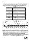
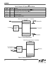
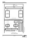
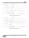
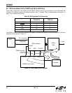
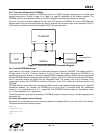
2.2.4.3. Parallel Interface Operation
When the device is powered up for parallel interface, the pins include eight data lines (D7–D0), a single address
(A0), a read strobe (RD
), a write strobe (WR), an interrupt line (INT), and chip select (CS). Table 23 summarizes
the parallel-interface signals:
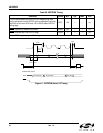
Refer to the device data sheet for timing characteristics. Address pin A0 allows the host processor to choose
between the two interface registers, HIR0 and HIR1. The timing diagrams below show typical parallel-interface
operation. Refer to the respective product data sheets for timing specifications.
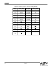
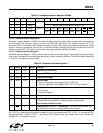
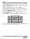
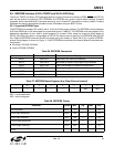
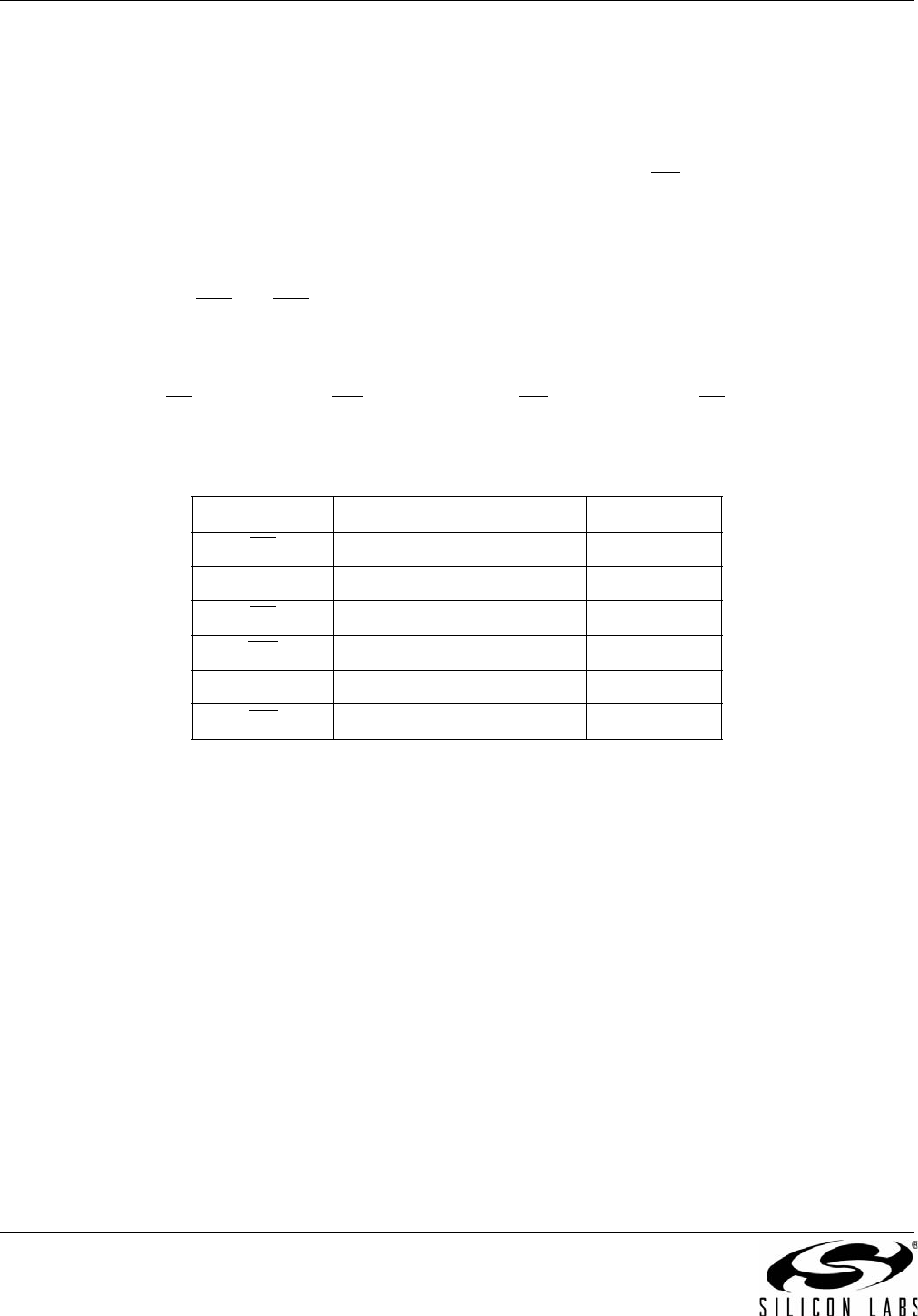
Table 23. Parallel Interface Signals
Signal Function Direction
CS
Chip Select (active low) Input
A0 Register address Input
RD
Read strobe (active low) Input
WR
Write strobe (active low) Input
D[7:0] Data bus Bidirectional
INT
Interrupt (active low) Output