


AN93
50 Rev. 1.3
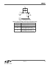
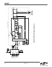
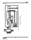
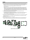
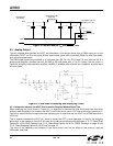
8. After the previous step, there should be some space between the grouping around U2 and the grouping of
components around the RJ11 jack. Place the rest of the components in this area, given the following guidelines:
a.Space U2, Q4, Q5, R1, R3, R4, R10 and R11 away from each other for best thermal performance.
b.The tightest layout can be achieved by grouping R6, C10, Q2, R3, R5, and Q1.
c.Place C3 next to D1.
d.Make the size of the Q1, Q3, Q4, and Q5 collector pads each sufficiently large for the transistor to safely
dissipate 0.5 W under worst case conditions. See the transistor data sheet for thermal resistance and
maximum operating temperature information. Implement collector pads on both the component and solder
side, and use vias between them to improve heat transfer for best performance. When ambient conditions
are a moderate 50 deg or less, use 0.05 square inches of copper at the collectors of Q1, Q3, Q4, Q5. Both
sides of the PCB can be used to double the available area.
9. U2, IGND, is the return path for many of the discrete components and requires special mention:
a.Traces associated with IGND should be 20 mils wide.
b.U2's IGND should not be a large ground plane and should only occupy the space under U2. Beyond this
area, use traces and avoid getting close to the components on the other side of the diode bridge.
c.C5, C6, C7 IGND return path should be direct.
10.The traces from R7 to FB1 and from R8 to FB2 should be well matched. This can be achieved by routing these
traces next to each other as much as possible. Ensure that these traces are not routed close to the traces
connected to C1 or C2.
11.Minimize all traces associated with Y1, C40, and C41.
12.Decoupling capacitors (0.22 µF and 0.1 µF capacitors connected to V
DA
, V
DB
, V
DD
) must be placed next to
those pins. Traces of these decoupling capacitors back to the Si24xx GND pin should be direct and short.
Figure 20. Reference Placement