


MZ-E800
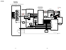
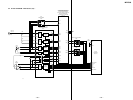
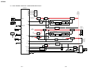
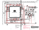
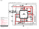
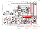
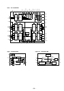
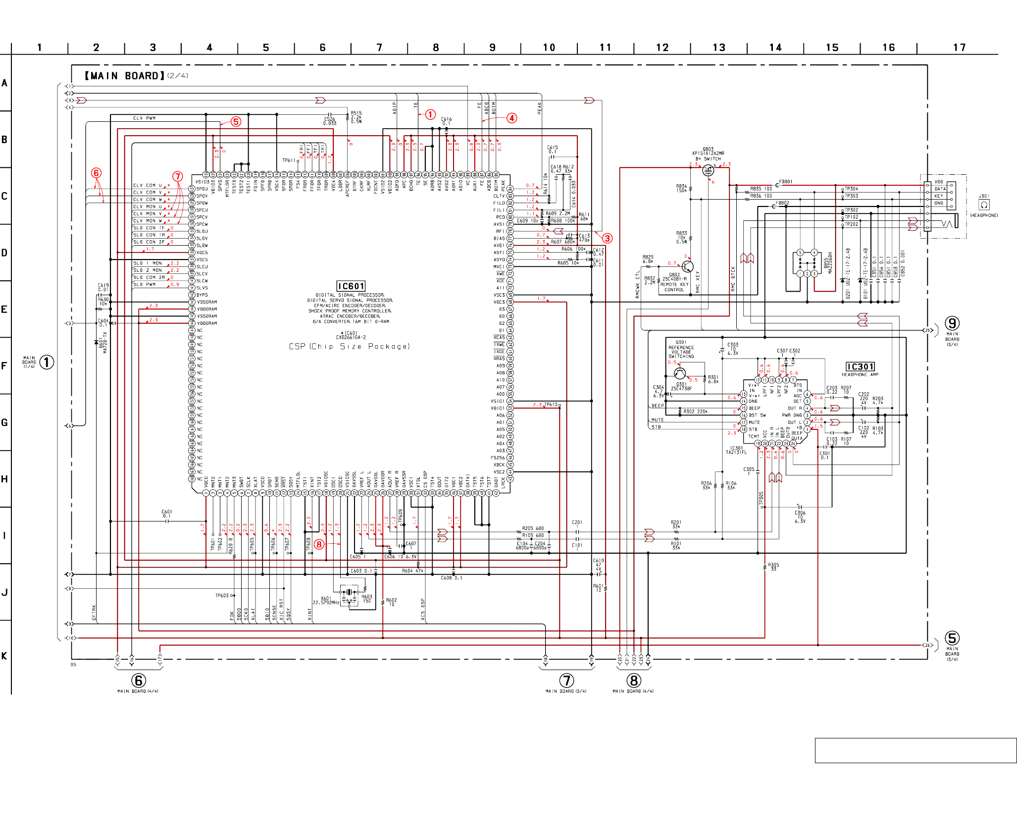
6-6. SCHEMATIC DIAGRAM – MAIN Board (2/4) –• See page 37 for Waveforms. • See page 38 for IC Block Diagram.
– 31 –
– 32 –
Note on Schematic Diagram:
• All capacitors are in µF unless otherwise noted. pF: µµF
50 WV or less are not indicated except for electrolytics
and tantalums.
• All resistors are in Ω and
1
/
4
W or less unless otherwise
specified.
• % : indicates tolerance.
•
f
: internal component.
• C : panel designation.
• A : B+ Line.
• Power voltage is dc 1.5V and fed with regulated dc power
supply from battery terminal.
• Voltages and waveforms are dc with respect to ground in
playback mode.
no mark : PLAYBACK
∗
: Impossible to measure
• Voltages are taken with a VOM (Input impedance 10 MΩ).
Voltage variations may be noted due to normal produc-
tion tolerances.
• Waveforms are taken with a oscilloscope.
Voltage variations may be noted due to normal produc-
tion tolerances.
• The voltage and waveform of CSP (chip size package)
cannot be measured, because its lead layout is different
form that of conventional IC.
* Replacement of IC601 used in this set requires a
special tool. Therefore, it cannnot be replaced.
• Circled numbers refer to waveforms.
• Signal path.
E : PLAYBACK
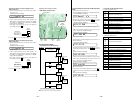
(Page 30)
(Page 36)
(Page 34)
(Page 36)
(Page 33)
(Page 33)