


– 41 –
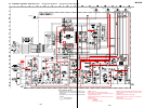
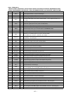
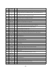
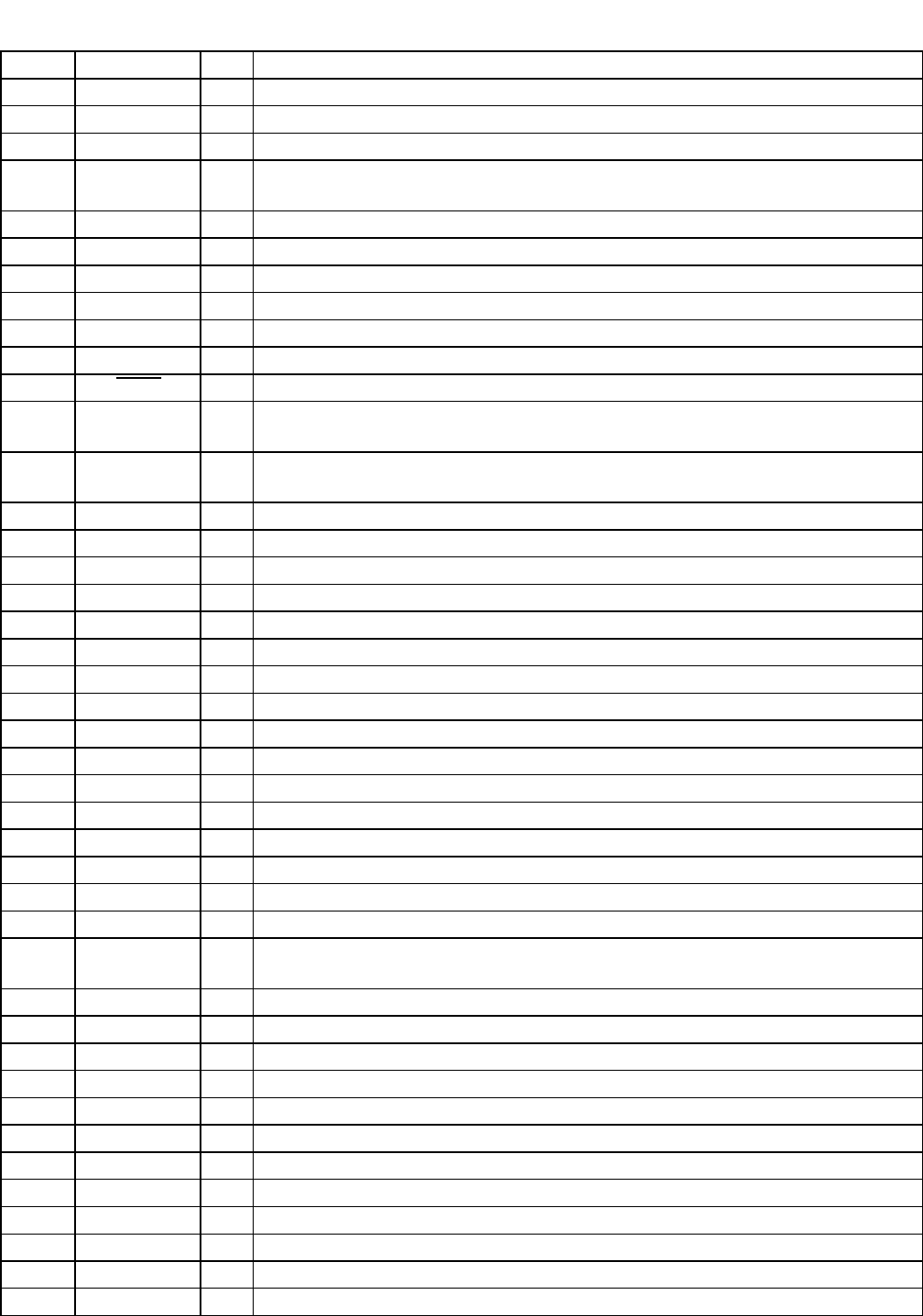
• IC601 CXD2661GA-2
Pin No. Pin Name I/O Description
1 VDCO — Power supply terminal (+1.7V) (for internal logic)
2, 3 MNT0, MNT1 O Operation monitor signal output terminal Not used (open)
4 MNT2 O Off track signal output to the SN761056CDBT (IC501) and system controller (IC801)
5 MNT3 O
Focus OK signal output to the system controller (IC801) “H” is output when focus is on
(“L”: NG)
6 SWDT I Serial data input from the system controller (IC801) and EEPROM (IC802)
7 SCLK I Serial clock signal input from the system controller (IC801)
8 XLAT I Serial data latch pulse input from the system controller (IC801)
9 VSCO — Ground terminal (for internal logic)
10 SRDT O Serial data output to the system controller (IC801) and EEPROM (IC802)
11 SENS O Internal status (SENSE) output to the system controller (IC801)
12 XRST I Reset signal input from the system controller (IC801) “L”: reset
13 SQSY O
Subcode Q sync (SCOR) output to the system controller (IC801)
“L” is output every 13.3 msec. Almost all, “H” is output
14 MTFLGL O
Muting applied to analog signal input in non-signal status causes the signal to be “H”
automatically Not used (open)
15 TST1 I Input terminal for the test (normally : fixed at “L”)
16 XINT O Interrupt status output to the system controller (IC801)
17 TST2 I Input terminal for the test (normally : fixed at “L”)
18 VDIOSC — Power supply terminal (+2.4V) (for oscillator cell)
19 OSCI I System clock input terminal (22.5792 MHz)
20 OSCO O System clock output terminal (22.5792 MHz)
21 VSIOSC — Ground terminal (for oscillator cell)
22 DAVSSL — Ground terminal (for internal D/A converter L-ch)
23 VREFL O Reference voltage output terminal (for internal D/A converter L-ch)
24 AOUTL O Playback analog signal (L-ch) output to the headphone amp (IC301)
25 DAVDDL — Power supply terminal (+2.4V) (for internal D/A converter L-ch)
26 DAVDDR — Power supply terminal (+2.4V) (for internal D/A converter R-ch)
27 AOUTR O Playback analog signal (R-ch) output to the headphone amp (IC301)
28 VREFR O Reference voltage output terminal (for internal D/A converter R-ch)
29 DAVSSR — Ground terminal (for internal D/A converter R-ch)
30 VSC1 — Ground terminal (for internal logic)
31 XTSL I
Input terminal for the system clock frequency setting
“L”: 45.1584 MHz, “H”: 22.5792 MHz (fixed at “H” in this set)
32 CD DSP I Chip select signal input from the system controller (IC801)
33 TST4 I Input terminal for the test (normally : fixed at “L”)
34 DOUT O Digital audio signal output terminal when playback mode Not used (open)
35 DT72 O Not used (open)
36, 37 VDC1, VDC2 — Power supply terminal (+1.7V) (for internal logic)
38 DATAI I Input terminal of external audio data to the internal D/A converter Not used (open)
39 to 41 TST5 to TST7 I Input terminal for the test (normally : fixed at “L”)
42 DADT O Playback data signal output to the external D/A converter Not used (open)
43 LRCK O L/R sampling clock signal (44.1 kHz) output to the external D/A converter Not used (open)
44 VSC2 — Ground terminal (for internal logic)
45 XBCK O Bit clock signal (2.8224 MHz) output to the external D/A converter Not used (open)
46 FS256 O Clock signal (11.2896 MHz) output to the external D/A converter Not used (open)
(DIGITAL SIGNAL PROCESSOR, DIGITAL SERVO SIGNAL PROCESSOR, EFM/ACIRC ENCODER/DECODER,
SHOCK PROOF MEMORY CONTROLLER, ATRAC ENCODER/DECODER, D/A CONVERTER, 16M BIT D-RAM)