


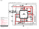
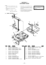
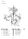
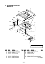
– 44 –
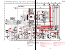
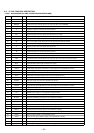
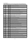
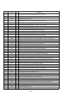
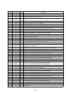
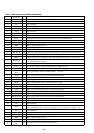
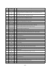
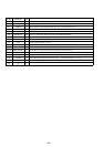
• IC801 CXR701080-016GA (SYSTEM CONTROLLER)
Pin No.
Pin Name
I/O Description
1
VLCD
O
Not used (open)
2
OFTRK
I
Off track signal input from the CXD2661GA (IC601)
3, 4
NC
I
Not used (open)
5
NC
O
Not used (open)
6 to 9 COM0 to COM3 O Common drive signal output to the liquid display module (LCD901)
10
NC
O
Not used (open)
11
SI0
I
Serial data input from the CXD2661GA (IC601)
12 SO0 O Serial data output to the CXD2661GA (IC601)
13 SCK0 O Serial clock signal output to the CXD2661GA (IC601) and EEPROM (IC802)
14 NC I Not used (open)
15 VSS
—
Ground terminal
16
VDD
—
Power supply terminal (+2.4V)
17
NC
O
Not used (open)
18
BEEP
O
Beep sound control signal output to the headphone amp (IC301)
19
RMC DTCK
I/O
TSB serial communication data input/output terminal for remote commander with headphone
20, 21
NC
O
Not used (open)
22
MUTE
O
Analog muting on/off control signal output to the headphone amp (IC301) “H”: muting on
23 XHP STBY O
Standby on/off control signal output to the headphone amp (IC301)
“L”: standby mode, “H”: amp on
24 CLV U
O
Spindle servo (U) drive signal input from the XC111256FTA (IC551)
25
CLV V
O
Spindle servo (V) drive signal input from the XC111256FTA (IC551)
26
CLV W
O
Spindle servo (W) drive signal input from the XC111256FTA (IC551)
27
XRST MTR
DRV
O
Reset signal output to the XC111256FTA (IC551) “L”: reset
28 XLAT O Serial data latch pulse signal output to the CXD2661GA (IC601)
29 XCS DSP O Chip select signal output to the CXD2661GA (IC601)
30 to 32
NC
O
Not used (open)
33 SENSE I Internal status (SENSE) input from the CXD2661GA (IC601)
34
TSB SLVE
I
Not used (fixed at “H”)
35
SLD MON 1
I
Sled servo timing signal input from the CXD2661GA (IC601)
36
PD S0
O
PD IC mode switching signal output to the optical pick-up block
37 NC O Not used (open)
38
PD S1
O
PD IC mode switching signal output to the optical pick-up block
39
RMC WK CTL
O
Starting signal output to the remote commander with headphone
40
XSLEEP
O
System sleep control signal output terminal “H”: sleep on
41
TSB EDGE
I
Not used (fixed at “L”)
42 NC O Not used (open)
43
XRST
I
System reset signal input from the reset signal generator (IC905) “L”: reset
For several hundreds msec. after the power supply rises, “L” is input, then it changes to “H”
44
VSS
—
Ground terminal
45 XTAL O
Main system clock output terminal (16.9344 MHz)
46 EXTAL I
Main system clock input terminal (16.9344 MHz)
47 VDD
—
Power supply terminal (+2.4V)
48 NC
I/O
Not used (open)
49
SPDL START
SW
O Spindle servo start switching signal output terminal