


10/100 Non-PCI Ethernet Single Chip MAC + PHY
Datasheet
Revision 1.91 (08-18-08) 62 SMSC LAN91C111 REV C
DATASHEET
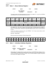
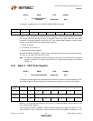
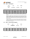
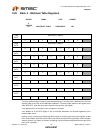
8.20 Bank 2 - Data Register
DATA REGISTER - Used to read or write the data buffer byte/word presently addressed by the pointer
register.
This register is mapped into two uni-directional FIFOs that allow moving words to and from the
LAN91C111 regardless of whether the pointer address is even, odd or dword aligned. Data goes
through the write FIFO into memory, and is pre-fetched from memory into the read FIFO. If byte
accesses are used, the appropriate (next) byte can be accessed through the Data Low or Data High
registers. The order to and from the FIFO is preserved. Byte, word and dword accesses can be mixed
on the fly in any order.
This register is mapped into two consecutive word locations to facilitate double word move operations
regardless of the actual bus width (16 or 32 bits). The DATA register is accessible at any address in
the 8 through Bh range, while the number of bytes being transferred is determined by A1 and nBE0-
nBE3. The FIFOs are 12 bytes each.
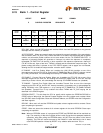
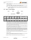
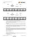
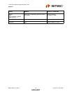
8.21 Bank 2 - Interrupt Status Registers
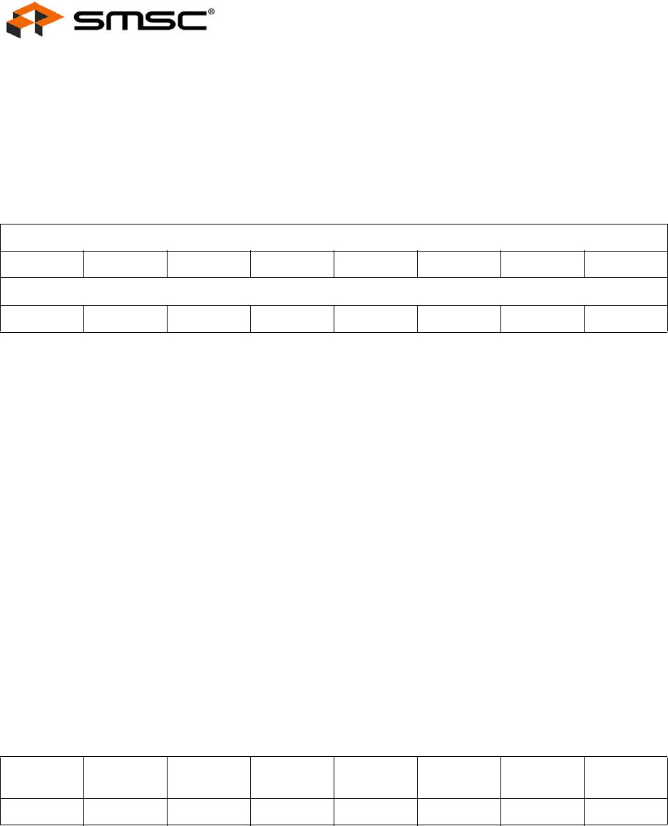
OFFSET NAME TYPE SYMBOL
8 THROUGH
BH DATA REGISTER READ/WRITE DATA
DATA HIGH
XXXXXXXX
DATA LOW
XXXXXXXX
OFFSET NAME TYPE SYMBOL
C
INTERRUPT STATUS
REGISTER READ ONLY IST
MDINT Reserved EPH INT RX_OVRN
INT
ALLOC INT TX EMPTY
INT
TX INT RCV INT
00000100