PCI-X v5.1 165 Getting Started Guide www.xilinx.com 23
UG158 March 24, 2008
Electrical Compliance
R
It is important to note that the frequency of this clock is not guaranteed to be constant. In
fact, in a compliant system, the clock may be any frequency, up to and including the
maximum allowed frequency, and the frequency may change on a cycle-by-cycle basis.
Under certain conditions, the PCI-X core may also apply phase shifts to this clock.
For these reasons, the user application should not use this clock as an input to a DLL or
PLL, nor should the user application use this clock in the design of interval timers (for
example, DRAM refresh counters).
Electrical Compliance
Virtex-II, Virtex-II Pro, and Virtex-4 devices, as specified in the relevant device data sheet,
exhibit a 10 pF pin capacitance. This is compliant with the PCI Local Bus Specification, with
one exception. The specification requires an 8 pF pin capacitance for the IDSEL pin, to
allow for non-resistive coupling to an AD[xx] pin. In practice, this coupling may be
resistive or non-resistive, and is performed on the system board or backplane. For system
board or backplane designs, use resistive coupling to avoid non-compliance. For add-in
cards, this is not under the control of the designer.
The PCI-X Addendum requires an 8 pF pin capacitance for all pins. Virtex-II, Virtex-II Pro,
and Virtex-4 devices do not comply with this requirement.
Although the core interface provides a direct PME# output from a general purpose I/O pin,
this output signal has certain limitations. If the FPGA power is removed, the general
purpose I/O pin will appear as a low impedance to ground. This appears to the system as
an assertion of PME#. For this reason, implementations that use the PME# signal should
employ an external buffering scheme that will prevent false assertions of PME# when
power is removed from the FPGA device.
For 3.3 volt signaling in Virtex-II Pro and Virtex-4 devices, the V
CCO
. supply must be
reduced to 3.0 volts and derived from a precision regulator. This reduction of the output
driver supply provides robust device protection without sacrificing PCI electrical
compliance, even in the extreme case where the 3.3 volt system supply climbs as high as
3.6 volts, as allowed by the PCI Local Bus Specification.
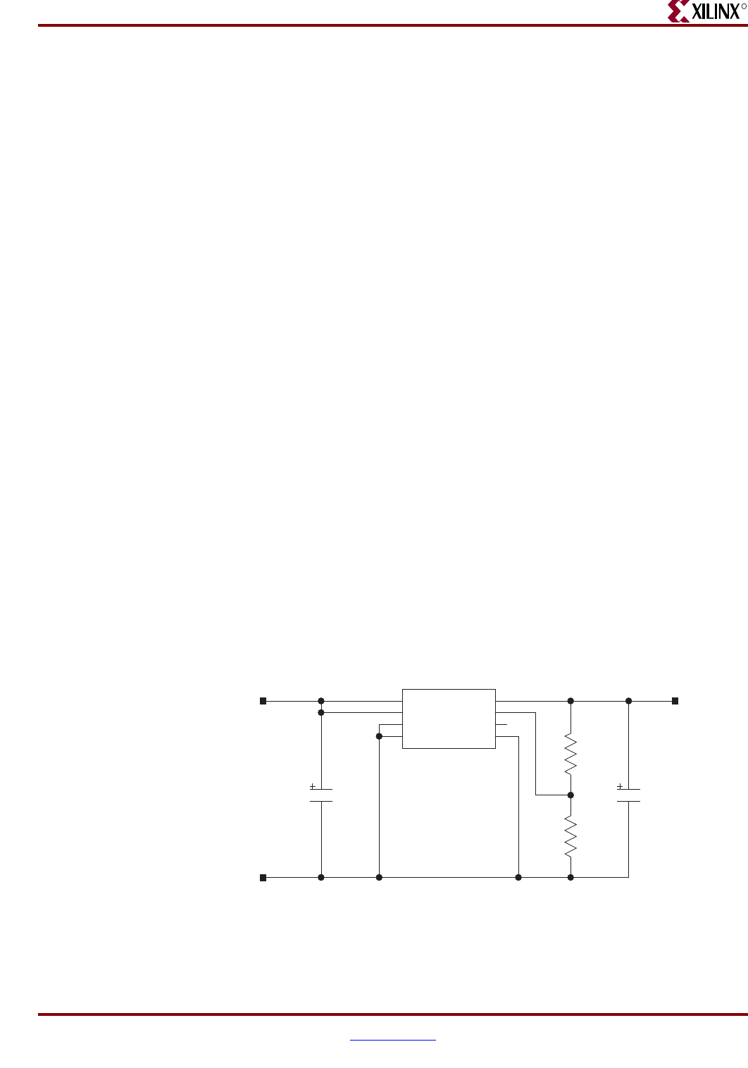
Figure 3-1 illustrates one possible low-cost solution to generate the required 3.0 volt output
driver supply. Xilinx recommends the use of this circuit; however, other approaches using
other regulators are possible.
Figure 3-1: PCI/PCI-X Output Driver VCCO Generation
GND
SUPPLY
+3.0V SUPPLY
26.1, 1%
1.0 uF
1
IN
GND
LT1763CS8
8
5
SHDN#
7
GND
6
OUT
ADJ
2
BYP
4
GND
33
4
2
6
7
5
10 uF
VCCO
38.3, 1%


