


ADSP-TS201S
Rev. C | Page 13 of 48 | December 2006
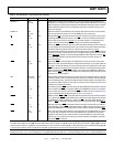
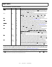
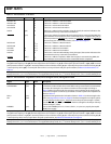
Table 5. Pin Definitions—External Port Bus Controls
Signal Type Term Description
ADDR31–0 I/O/T
(pu_ad)
nc Address Bus. The DSP issues addresses for accessing memory and peripherals on
these pins. In a multiprocessor system, the bus master drives addresses for accessing
internal memory or I/O processor registers of other ADSP-TS201S processors. The DSP
inputs addresses when a host or another DSP accesses its internal memory or I/O
processor registers.
DATA63–0 I/O/T
(pu_ad)
nc External Data Bus. The DSP drives and receives data and instructions on these pins.
Pull-up or pull-down resistors on unused DATA pins are unnecessary.
RD
I/O/T
(pu_0)
epu
1
Memory Read. RD is asserted whenever the DSP reads from any slave in the system,
excluding SDRAM. When the DSP is a slave, RD
is an input and indicates read trans-
actions that access its internal memory or universal registers. In a multiprocessor
system, the bus master drives RD. RD changes concurrently with ADDR pins.
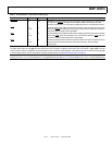
WRL
I/O/T
(pu_0)
epu
1
Write Low. WRL is asserted in two cases: when the ADSP-TS201S processor writes to
an even address word of external memory or to another external bus agent; and when
the ADSP-TS201S processor writes to a 32-bit zone (host, memory, or DSP
programmed to 32-bit bus). An external master (host or DSP) asserts WRL
for writing
to a DSP’s low word of internal memory. In a multiprocessor system, the bus master
drives WRL
. WRL changes concurrently with ADDR pins. When the DSP is a slave, WRL
is an input and indicates write transactions that access its internal memory or
universal registers.
WRH
I/O/T
(pu_0)
epu
1
Write High. WRH is asserted when the ADSP-TS201S processor writes a long word
(64 bits) or writes to an odd address word of external memory or to another external
bus agent on a 64-bit data bus. An external master (host or another DSP) must assert
WRH
for writing to a DSP’s high word of 64-bit data bus. In a multiprocessing system,
the bus master drives WRH
. WRH changes concurrently with ADDR pins. When the
DSP is a slave, WRH is an input and indicates write transactions that access its internal
memory or universal registers.
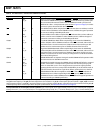
ACK I/O/T/OD
(pu_od_0)
epu
1
Acknowledge. External slave devices can deassert ACK to add wait states to external
memory accesses. ACK is used by I/O devices, memory controllers, and other periph-
erals on the data phase. The DSP can deassert ACK to add wait states to read and write
accesses of its internal memory. The pull-up is 50 Ω on low-to-high transactions and
is 500 Ω on all other transactions.
BMS
O/T
(pu_0)
na Boot Memory Select. BMS is the chip select for boot EPROM or flash memory. During
reset, the DSP uses BMS
as a strap pin (EBOOT) for EPROM boot mode. In a multipro-
cessor system, the DSP bus master drives BMS
. For details, see Reset and Booting on
Page 9 and the EBOOT signal description in Table 16 on Page 20.
MS1–0
O/T
(pu_0)
nc Memory Select. MS0 or MS1 is asserted whenever the DSP accesses memory banks 0
or 1, respectively. MS1–0
are decoded memory address pins that change concurrently
with ADDR pins. When ADDR31:27 = 0b00110, MS0
is asserted. When ADDR31:27 =
0b00111, MS1 is asserted. In multiprocessor systems, the master DSP drives MS1–0.
MSH
O/T
(pu_0)
nc Memory Select Host. MSH is asserted whenever the DSP accesses the host address
space (ADDR31 = 0b1). MSH
is a decoded memory address pin that changes concur-
rently with ADDR pins. In a multiprocessor system, the bus master DSP drives MSH
.
BRST
I/O/T
(pu_0)
epu
1
Burst. The current bus master (DSP or host) asserts this pin to indicate that it is reading
or writing data associated with consecutive addresses. A slave device can ignore
addresses after the first one and increment an internal address counter after each
transfer. For host-to-DSP burst accesses, the DSP increments the address automati-
cally while BRST
is asserted.
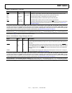
I = input; A = asynchronous; O = output; OD = open-drain output; T = three-state; P = power supply; G = ground; pd = internal pull-down
5k
Ω; pu = internal pull-up 5 kΩ; pd_0 = internal pull-down 5 kΩ on DSP ID = 0; pu_0 = internal pull-up 5 kΩ on DSP ID = 0; pu_od_0 = internal
pull-up 500
Ω on DSP ID = 0; pd_m = internal pull-down 5 kΩ on DSP bus master; pu_m = internal pull-up 5 kΩ on DSP bus master; pu_ad
= internal pull-up 40 k
Ω. For more pull-down and pull-up information, see Electrical Characteristics on Page 22.
Term (termination of unused pins) column symbols: epd = external pull-down approximately 5 k
Ω to V
SS
; epu = external pull-up approx-
imately 5 k
Ω to V
DD_IO
, nc = not connected; na = not applicable (always used); V
DD_IO
= connect directly to V
DD_IO
; V
SS
= connect directly to V
SS
1
This external pull-up may be omitted for the ID = 000 TigerSHARC processor.